MT90222 Просмотр технического описания (PDF) - Zarlink Semiconductor Inc
Номер в каталоге
Компоненты Описание
производитель
MT90222 Datasheet PDF : 155 Pages
| |||
MT90222/3/4
Data Sheet
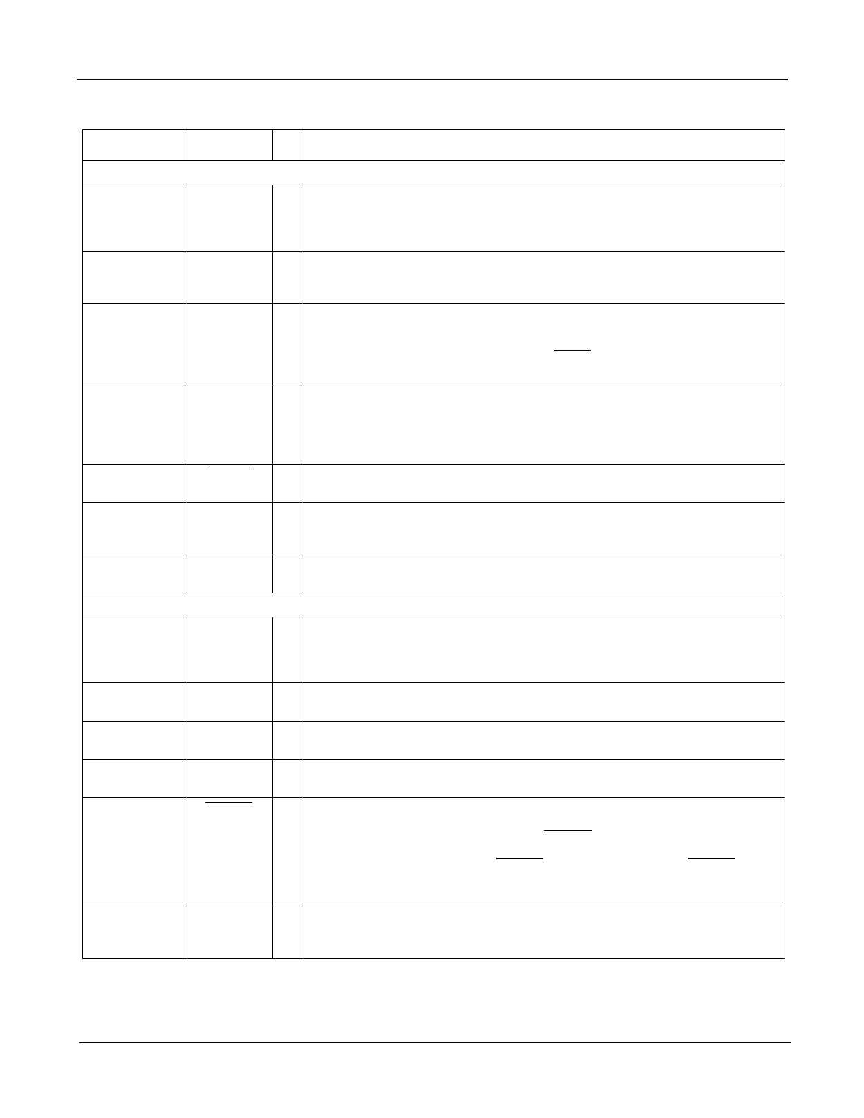
MT90223 Pin Description
Pin #
Name
U2,U1,T4,T2,
T1,R3,R4,R2,
R1,P3,P1,N1,
N2,N3,M2,M4
U3
UTxData
[15:0]
UTxPar
V1
UTxSOC
V4
UTxClk
V3
UTxEnb
V2
UTxClav
Y4,W3,W4,
W2,W1
UTxAddr
[4:0]
H3,H4,G1,G2,G
3,G4,F1,F2,
F3,E1,E3,D1,
D2,C1,D3,C2
H2
URxData
[15:0]
URxPar
J4
URxSOC
K3
URxClk
K2
URxEnb
J3
URxClav
I/O
Description
ATM Input Port Signals (UTOPIA Transmit Interface)
I UTOPIA Transmit Data Bus. 16 (or 8) bit wide data driven from ATM LAYER device
to MT90223. Bit 15 (or 7) is the MSB. All arriving data between the last word (byte) of
the previous cell and the first word (byte) of the following cell (indicated by the SOC
signal) is ignored. UTxData[15:8] have internal weak pull-downs.
I UTOPIA Transmit Parity. Odd (or Even) Parity bit generated by the ATM LAYER. The
parity bit is sampled on the rising edge of UTxClk. UTxPar has an internal weak
pull-down.
I UTOPIA Transmit Start of Cell Signal. Active HIGH signal asserted by the ATM
LAYER device when TxData[15:0] ([7:0]) contains the first valid word (byte) of the cell.
After this signal is high, the following 26 word (52 bytes) should contain valid data.
The MT90223 waits for another TxSOC and TxEnb signal after reading a complete
cell.An external pull-down (4.7 K) is strongly recommended.
I UTOPIA Transmit Clock. Transfer clock from the ATM Layer device to the MT90223
which synchronizes data transfers on TxData[15:0] ([7:0]). This signal is the clock of
the incoming data. Data is sampled on the rising edge of this signal.For 8-bit UTOPIA
mode the maximum supported clock is 52 MHz and for 16-bit UTOPIA mode
maximum supported clock is 33 MHz.
I UTOPIA Transmit Data Enable. Active LOW signal asserted by the ATM LAYER
device during cycles when TxData contains valid cell data.
O UTOPIA Transmit Cell Available Signal. For cell-level flow control in a MPHY
environment, TxClav is an active high tri-stateable signal from the MT90223 to the
ATM LAYER device.
I Transmit Address. Five bit wide address bus driven by the ATM layer device to poll
and select the appropriate PHY address. TxAddr[4] is the MSB.
ATM Output Port Signals (UTOPIA Receive Interface)
O UTOPIA Receive Data Bus. 16 (or 8) bit wide data driven from MT90223 to ATM
layer device. RxData[15] ([7]) is the MSB. To support multiple PHY configurations,
RxData is driven only when RxEnb and port is selected. It is tri-stated otherwise.
O UTOPIA Receive Parity. Odd (or Even) Parity bit generated by the MT90223 to the
ATM Layer.
O UTOPIA Receive Start of Cell Signal. Active high asserted by the MT90223 when
RxData contains the first valid word (byte) of a cell.
I UTOPIA Receive Clock. This signal is the clock driven from the ATM layer to the
PHY layer. Data changes after the rising edge of this signal.
I UTOPIA Receive Data Enable. Active LOW signal asserted by the ATM layer device
to indicate that URxData[15:0] ([7:0]) and URxSOC will be sampled at the end of the
next cycle. In multiple PHY configurations, URxEnb is used to tri-state URxData and
URxSOC MT90223 outputs. In this case, URxData and URxSOC would be enabled
only in cycles following those with URxEnb asserted. In UTOPIA L1, URxEnb must
not be tied low and must transition from high (disabled) to low (enabled) to indicate
the beginning of data transfer.
O UTOPIA Receive Cell Available Signal. For cell-level flow control in a MPHY
environment, URxClav is an active high tri-stateable signal from the MT90223 to ATM
LAYER device.
20
Zarlink Semiconductor Inc.
Share Link: 