MT90222 Просмотр технического описания (PDF) - Zarlink Semiconductor Inc
Номер в каталоге
Компоненты Описание
производитель
MT90222 Datasheet PDF : 155 Pages
| |||
MT90222/3/4
Data Sheet
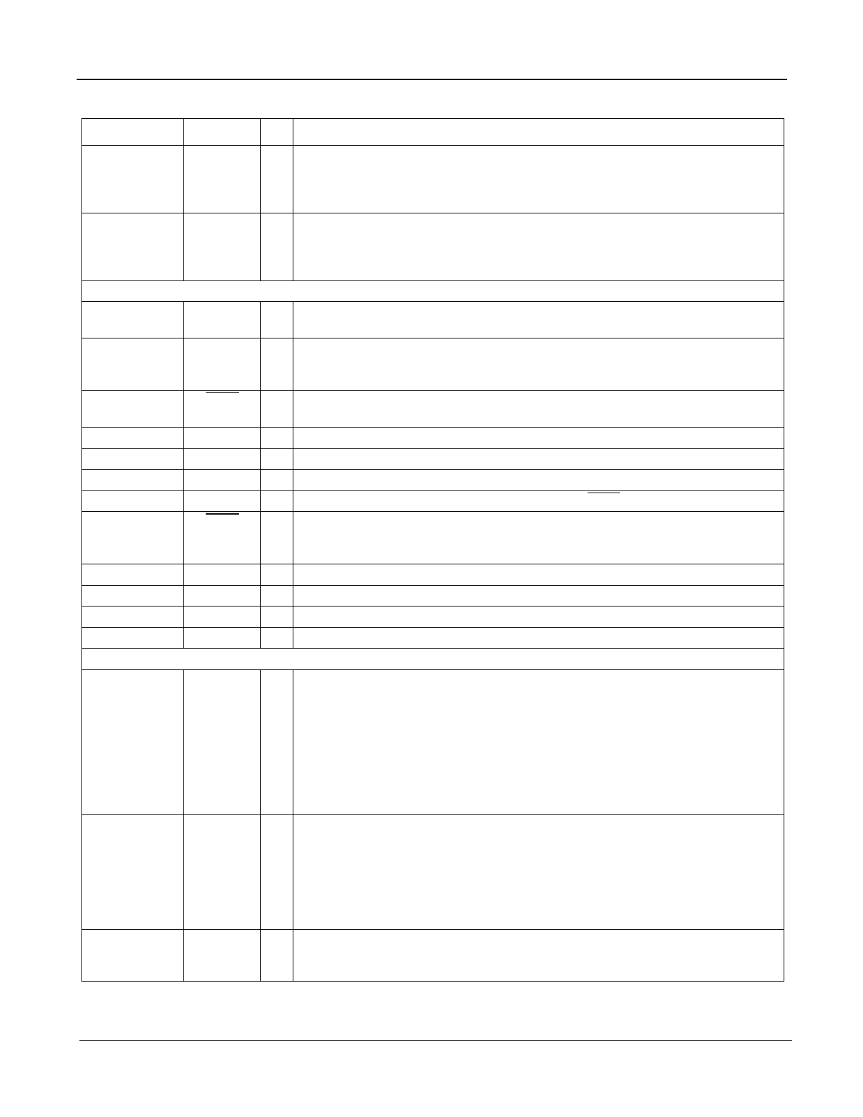
MT90222 Pin Description (continued)
Pin #
Name I/O
Description
AF14
RXRing
Sync
I TDM Ring RX Sync. Synchronization input signal used to retrieve data and control
from the bytes on RXRingData. Should be connected to the TXRingSync output of the
previous MT90222 device in the Ring. There is an internal weak pull-down on this
input. NOT 5 V TOLERANT.
AC16,AE16,
AF16,AC15,
AE15,AF15,
AD14,AE14
RXRing
Data[7:0]
I TDM Ring RX Data[7:0]. Data Bus connecting the RX TDM Ring port to the TX TDM
Ring port. Should be connected to the TXRingData inputs of the previous MT90222
device in the Ring. There are internal weak pull-downs on these inputs. NOT 5 V
TOLERANT.
System Signals
AC1
Clk
I System Clock (50 MHz nominal). In the MT90222, this clock is used for all internal
operations of the device.
C19
LatchClk I Counter Latch Clock. The clock present at this input can be divided internally to
produce the latch signal for the internal counters. Refer to the Counter Transfer
Command register for more details. This pin has an internal pull-down.
A4
Reset
I System Reset. This is an active low input signal. It causes the device to enter the
initial state. The Clk signal must be active to reset the internal registers.
D7
TCK
I JTAG Test Clock. TCK should be pulled down if not used.
A5
TMS
I JTAG Test Mode Select. TMS is sampled on the rising edge of TCK.
B6
TDI
I JTAG Test Data Input. This pin has an internal weak pull-down.
C6
TDO
O JTAG Test Data Output. Note: TDO is tristated by TRST pin.
B5
TRST
I JTAG Test Reset (active low). Should be asserted LOW on power-up and during
reset. Must be HIGH for JTAG boundary-scan operation. This pin has an internal weak
pull-down.
AD1
Test1
I Test1. Must be tied Low
D19
Test2
O Test2. Must be left not connected (NC).
C7
Test3
I Test3. Must be pulled up to V3.3 for normal operation. NOT 5 V TOLERANT.
B4
Test4
O Test4. Must be left not connected (NC)
Power Signals
E2,H1,J1,M3,
P2,T3,Y2,AB3,
AE6,AF8,
AD12,AD15,
AC19,AD25,
AA25,V26,
N25,H26,F26,A
23,D20,C16,A1
3,A8,C5
VDD5
S 5 Volt supply pin. Connect to a 5 volt supply when interfacing to 5 volt signals,
otherwise, connect to a 3.3 Volt supply.
AA23,AB04,
AC06,AC13,
AC17,AC22,
D6,D10,D14,
D22,E23,F4,
K23,N4,P23,
U4
V3.3
S 3.3 Volt supply pin for I/O pins. Connect to a 3.3 Volt supply.
D13,D17,N23,U
23,AC10,
AC14,K4,P4
V2.5
S 2.5 Volt supply for core. Connect to a 2.5 Volt power supply.
17
Zarlink Semiconductor Inc.
Share Link: 