SAA3323 Просмотр технического описания (PDF) - Philips Electronics
Номер в каталоге
Компоненты Описание
производитель
SAA3323 Datasheet PDF : 56 Pages
| |||
Philips Semiconductors
Drive processor for DCC systems
Preliminary specification
SAA3323
A simplified block diagram of the SAA3323 is shown in
Fig.1.
DCC drive processing
The SAA3323 provides the following functions for the DCC
drive processing.
PLAYBACK MODES
• Analog-to-digital conversion
• Tape channel equalization
• Tape channel data and clock recovery
• 10-to-8 demodulation
• Data placement in system RAM
• C1 and C2 error correction decoding
• Interfacing to sub-band serial PASC interface
• Interfacing to microcontroller for SYSINFO and AUX
data
• Capstan control for tape deck.
RECORD MODES
• Interfacing to sub-band serial PASC interface
• C1 and C2 error correction encoding
• Formatting for tape transfer
• 8-to-10 modulation
• Interfacing to microcontroller for SYSINFO and AUX
data
• Capstan control for tape deck, programmable by
microcontroller.
SEARCH MODE
• Detection and interpretation of AUX envelope
information
• AUX envelope counting
• Search speed estimation.
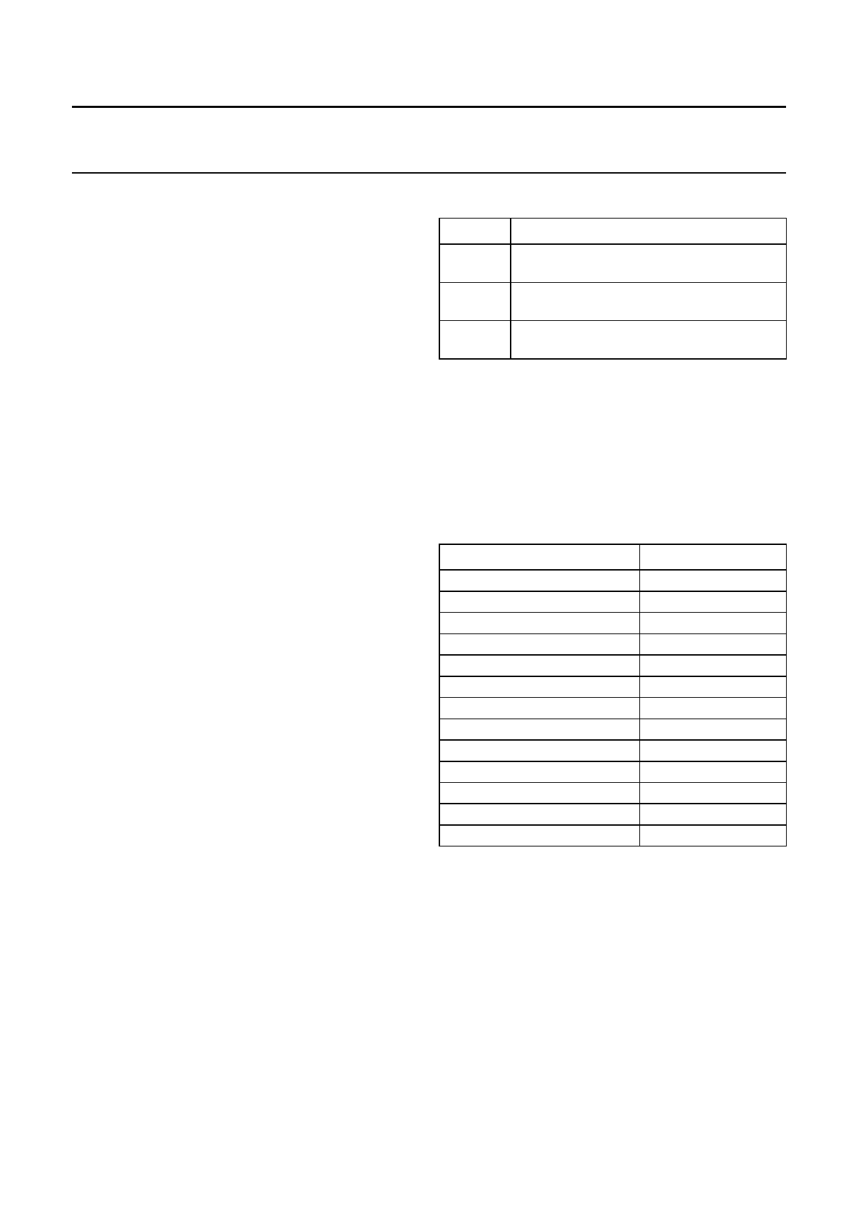
Tape Formatting and Error (TFE) correction module
The TFE module has 3 basic modes of operation as shown
in Table 1.
Table 1 Basic modes of TFE module.
MODE
DPAP
DPAR
DRAR
EXPLANATION
audio and SYSINFO (main data) play;
AUX play
audio and SYSINFO (main data) play;
AUX record
audio and SYSINFO (main data) record;
AUX record
TFE REGISTERS
The TFE module has 8 writable and 5 readable registers
that are accessible via the L3 interface, one write register
(CMD) and four read registers (STATUS0 to STATUS3)
which are directly addressable, the other registers are
indirectly addressable via commands sent to the CMD
register. The registers are named as shown in Table 2.
Table 2 TFE register names.
REGISTER NAME
CMD
STATUS0
STATUS1
STATUS2
STATUS3
SET0
SET1
SET2
SET3(1)
SPDDTY
BYTCNT
RACCNT
SPEED
READ/WRITE
W
R
R
R
R
W
W
W
W
W
W
W
R
Note
1. The 4 LSBs of register ‘SET3’ set RAM type (RType)
and RAM timing (RTim). See Table 3.
For normal operation the 4 MSBs of register ‘SET3’
should be logic 0.
May 1994
9
Share Link: 