IRF7469TRPBF Просмотр технического описания (PDF) - VBsemi Electronics Co.,Ltd
Номер в каталоге
Компоненты Описание
производитель
IRF7469TRPBF Datasheet PDF : 9 Pages
| |||
IRF7469TRPBF
www.VBsemi.tw
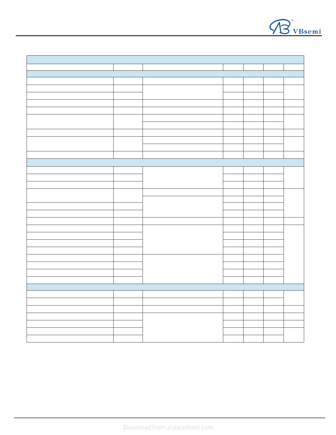
SPECIFICATIONS TJ = 25 °C, unless otherwise noted
Parameter
Symbol
Test Conditions
Static
Drain-Source Breakdown Voltage
VDS
VGS = 0 V, ID = 250 µA
VDS Temperature Coefficient
VGS(th) Temperature Coefficient
Gate-Source Threshold Voltage
ΔVDS/TJ
ΔVGS(th)/TJ
VGS(th)
ID = 250 µA
VDS = VGS , ID = 250 µA
Gate-Source Leakage
IGSS
VDS = 0 V, VGS = ± 20 V
Zero Gate Voltage Drain Current
On-State Drain Currenta
IDSS
ID(on)
VDS = 40 V, VGS = 0 V
VDS = 40 V, VGS = 0 V, TJ = 55 °C
VDS ≥ 5 V, VGS = 10 V
Drain-Source On-State Resistancea
Forward Transconductancea
RDS(on)
gfs
VGS = 10 V, ID = 12.4 A
VGS = 4.5 V, ID = 10.8 A
VDS = 15 V, ID = 12.4 A
Dynamicb
Input Capacitance
Ciss
Output Capacitance
Coss
VDS = 20 V, VGS = 0 V, f = 1 MHz
Reverse Transfer Capacitance
Crss
Total Gate Charge
Qg
VDS = 10 V, VGS = 10 V, ID = 12.4 A
Gate-Source Charge
Qgs
Gate-Drain Charge
Qgd
Gate Resistance
Rg
Turn-On Delay Time
td(on)
Rise Time
tr
Turn-Off Delay Time
td(off)
Fall Time
tf
Turn-On Delay Time
td(on)
Rise Time
tr
Turn-Off Delay Time
td(off)
Fall Time
tf
Drain-Source Body Diode Characteristics
Continuous Source-Drain Diode Current
IS
Pulse Diode Forward Current
ISM
Body Diode Voltage
VSD
Body Diode Reverse Recovery Time
trr
Body Diode Reverse Recovery Charge
Qrr
Reverse Recovery Fall Time
ta
Reverse Recovery Rise Time
tb
Notes:
a. Pulse test; pulse width ≤ 300 µs, duty cycle ≤ 2 %
b. Guaranteed by design, not subject to production testing.
VDS = 10 V, VGS = 4.5 V, ID = 12.4 A
f = 1 MHz
VDD = 20 V, RL = 2 Ω
ID ≅ 10 A, VGEN = 4.5 V, Rg = 1 Ω
VDD = 20 V, RL = 2 Ω
ID ≅ 10 A, VGEN = 10 V, Rg = 1 Ω
TC = 25 °C
IS = 10 A, VGS = 0 V
IF = 10 A, dI/dt = 100 A/µs, TJ = 25 °C
Min.
40
1
50
Typ.
40
-6
0.010
0.012
56
2000
260
150
33
15
6.7
5.1
1.4
25
12
25
10
10
15
30
10
0.8
30
26
17.5
12.5
Max. Unit
V
mV/°C
3
V
± 100
nA
1
µA
5
A
Ω
S
pF
50
23
nC
2.1
Ω
40
20
40
15
ns
15
25
45
15
30
A
50
1.2
V
60
ns
52
nC
ns
Stresses beyond those listed under “Absolute Maximum Ratings” may cause permanent damage to the device. These are stress ratings only, and functional operation
of the device at these or any other conditions beyond those indicated in the operational sections of the specifications is not implied. Exposure to absolute maximum
rating conditions for extended periods may affect device reliability.
E-mail:China@VBsemi TEL:86-755-83251052
2
Share Link: 