MAX3674 Просмотр технического описания (PDF) - Microsemi Corporation
Номер в каталоге
Компоненты Описание
производитель
MAX3674 Datasheet PDF : 20 Pages
| |||
High-Performance, Dual-Output,
Network Clock Synthesizer
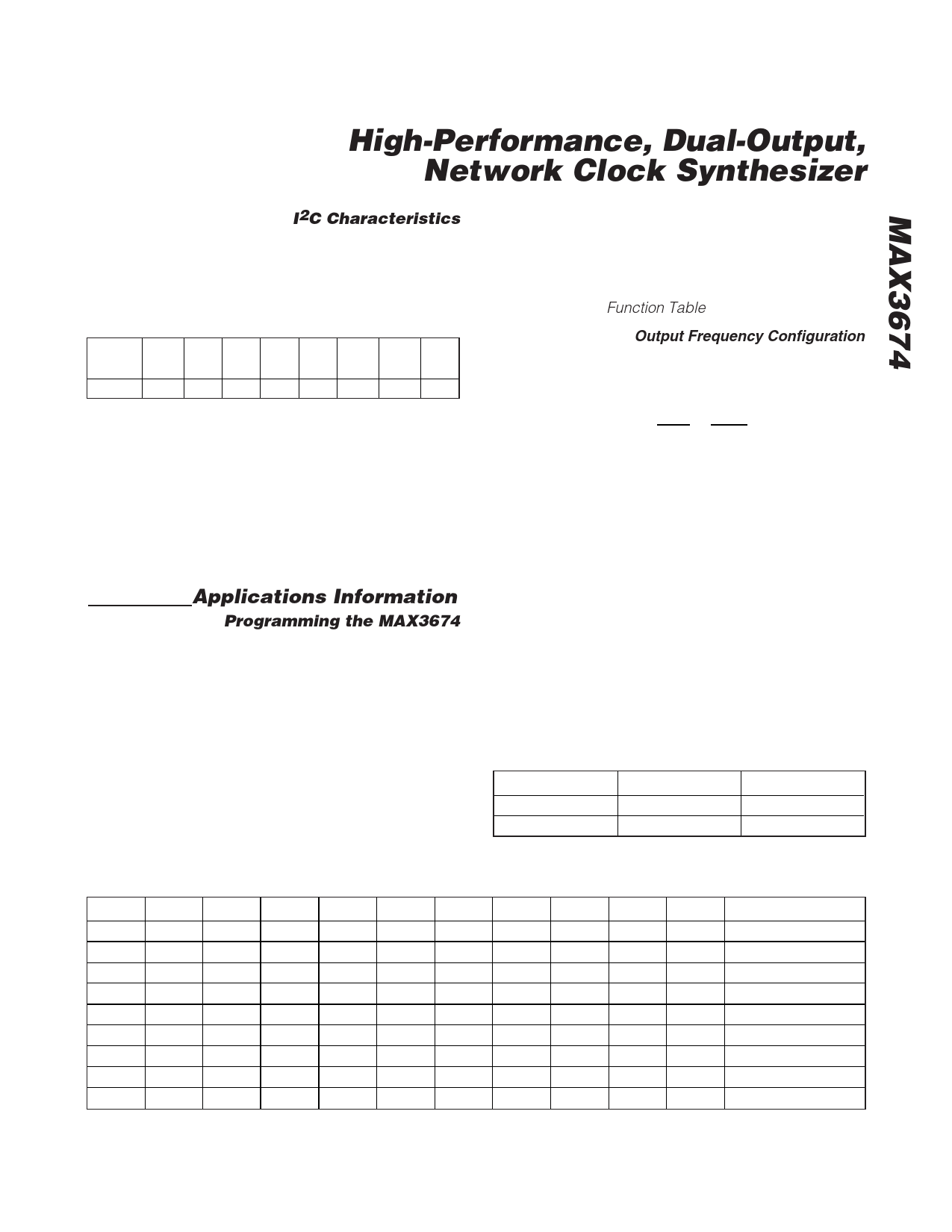
I2C Characteristics
The MAX3674 acts as a slave device on the I2C bus
supporting fast-mode data transfer (up to 400kbps). Its
clock pin, SCL, is an input only. It does not support
clock stretching. Table 3 shows the I2C slave address.
Table 3. I2C Slave Address
BIT
7
(MSB)
6
5
4
3
2
1
0
(LSB)
VALUE 1 0 1 1 0 ADR1 ADR0 R/W
The slave address is composed of a 5-bit fixed address
and 2-bit variable address that is set by the input pins
ADR[1:0]. The variable address pins are used to avoid
address conflicts of multiple MAX3674 devices on the
same I2C bus.
The host controller uses bit 0 (LSB) of the MAX3674
slave address to select either read or write mode. “0”
indicates I2C “write” to the MAX3674 registers; “1” indi-
cates I2C “read” from the MAX3674 registers.
Applications Information
Programming the MAX3674
The MAX3674 PLL configurations can be controlled
either through the parallel interface or the serial I2C
interface. The parallel interface allows the user to
directly configure the PLL dividers through hardwired
pins without the overhead of a serial interface. At
device startup, the device always obtains an initial PLL
frequency configuration through the parallel interface.
The PLL configuration can be read through I2C in paral-
lel interface mode.
The serial interface is I2C compatible. It allows reading
and writing device settings through built-in registers. It
also allows a host controller to program the output
frequency of the synthesizer on the fly using the incre-
ment and decrement functions for frequency margining
applications.
An LVCMOS-compatible input (PLOAD) is used to
select the parallel interface or serial interface, as
described in the Function Table.
Output Frequency Configuration
The MAX3674 output frequency (fOUT) is a function of
the reference frequency (fREF) and the programmable
dividers (P, M, and NA,B) and is expressed as:
fOUT =
fREF
P
×
M
N A,B
The numbers P, M, NA, and NB are divider ratios
requiring configuration through parallel programming or
I2C serial interfaces using registers PLL_L and PLL_H.
P is the predivider to the input of the phase-locked loop
(PLL) and has a valid division ratio of 2 or 4 (Table 4). P
can be set by the parallel interface pin P or through the
serial I2C interface. M is determined by the inputs at the
10-pin M[9:0] through parallel interface or by program-
ming through the serial I2C interface (Table 5). NA
determines the postdivider for differential output QA
and QB, and has a valid division value of 2, 4, 8, 16,
32, or 64 based on the 3-pin inputs NA[2:0] (Table 6).
NA can also be set through the serial I2C interface. NB
is the postdivider for output QB and has a valid value of
1 or 2 (Table 7). NB can be set by the parallel interface
pin NB or through the serial I2C interface.
Table 4. Pre-PLL Divider P
P
VALUE
0
fREF / 2
1
fREF / 4
DEFAULT VALUE
—
1
Table 5. PLL Feedback Divider M
M[9:0] M9
M8
M7
M6
M5
M4
M3
M2
M1
M0
DEFAULT VALUE
136
0
0
1
0
0
0
1
0
0
0
—
137
0
0
1
0
0
0
1
0
0
1
—
...
—
500
0
1
1
1
1
1
0
1
0
0
01 1111 0100
...
—
512
1
0
0
0
0
0
0
0
0
0
—
...
—
724
1
0
1
1
0
1
0
1
0
0
—
725
1
0
1
1
0
1
0
1
0
1
—
______________________________________________________________________________________ 11
Share Link: 