ADSP-21065L Просмотр технического описания (PDF) - Analog Devices
Номер в каталоге
Компоненты Описание
производитель
ADSP-21065L Datasheet PDF : 44 Pages
| |||
ADSP-21065L
Synchronous Read/Write—Bus Slave
Use these specifications for ADSP-21065L bus master accesses of a slave’s IOP registers or internal memory (in multiprocessor
memory space). The bus master must meet these (bus slave) timing requirements.
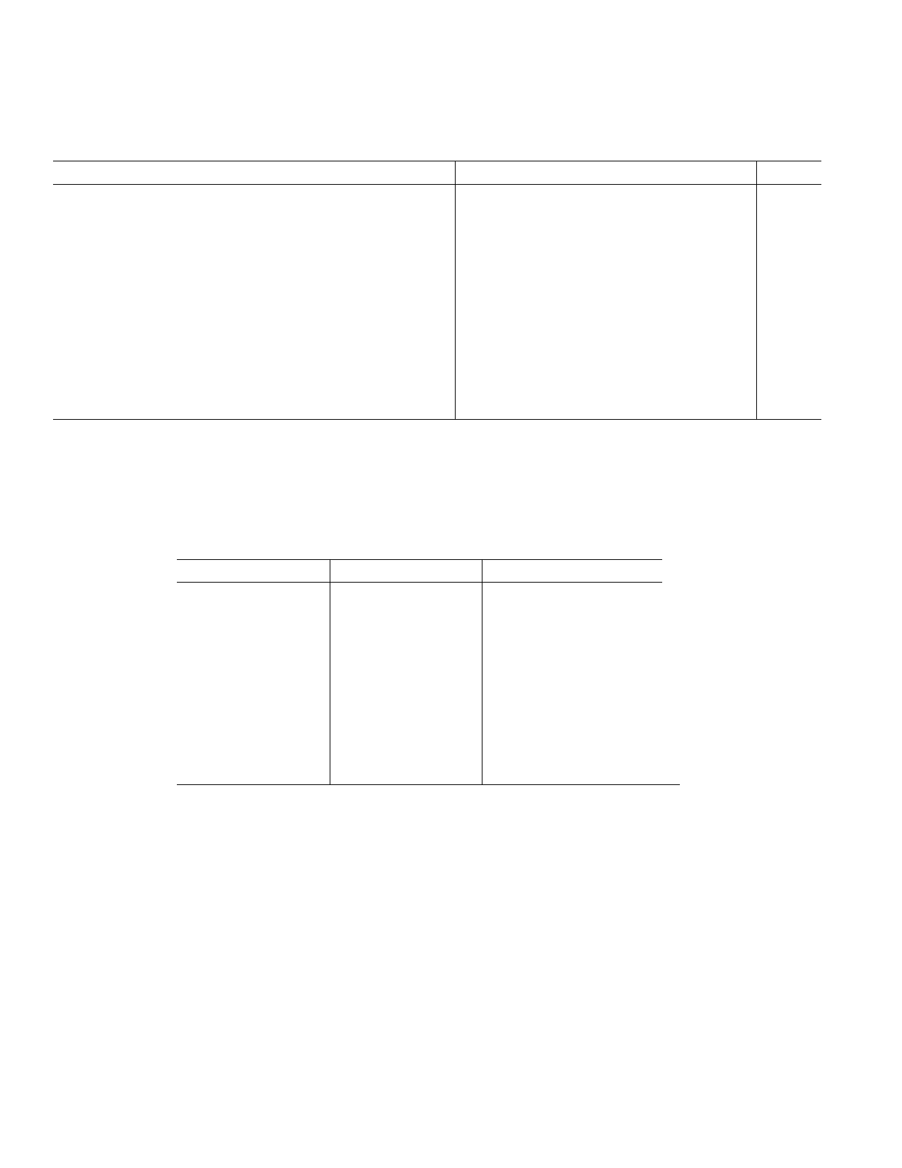
Parameter
Timing Requirements:
tSADRI
tHADRI
tSRWLI
tHRWLI
tRWHPI
tSDATWH
tHDATWH
Address, SW Setup Before CLKIN
Address, SW Hold Before CLKIN
RD/WR Low Setup Before CLKIN1
RD/WR Low Hold After CLKIN
RD/WR Pulse High
Data Setup Before WR High
Data Hold After WR High
Min
24.5 + 25 DT
21.0 + 21 DT
–2.50 – 5 DT
2.5
4.5
0.0
Max
4.0 + 8 DT
7.5 + 7 DT
Unit
ns
ns
ns
ns
ns
ns
ns
Switching Characteristics:
tSDDATO
tDATTR
tDACK
tACKTR
Data Delay After CLKIN
Data Disable After CLKIN2
ACK Delay After CLKIN
ACK Disable After CLKIN2
1.0 – 2 DT
1.0 – 2 DT
31.75 + 21 DT
ns
7.0 – 2 DT
ns
29.5 + 20 DT
ns
6.0 – 2 DT
ns
NOTES
1tSRWLI is specified when Multiprocessor Memory Space Wait State (MMSWS bit in WAIT register) is disabled; when MMSWS is enabled, tSRWLI (min) = 17.5 + 18 DT.
2See System Hold Time Calculation under Test Conditions for calculation of hold times given capacitive and dc loads.
For two ADSP-21065Ls to communicate synchronously as master and slave, certain master and slave specification combinations
must be satisfied. Do not compare specification values directly to calculate master/slave clock skew margins for those specifications
listed below. The following table shows the appropriate clock skew margin.
Table IV. Bus Master to Slave Skew Margins
Master Specification
tSSDATI
tSACKC
tDADRO
tDRWL (Max)
tDRDO (Max)
tDWRO (Max)
Slave Specification
tSDDATO
tDACK
tSADRI
tSRWLI
tHRWLI (Max)
tHRWLI (Max)
Skew Margin
tCK = 33.3 ns
tCK = 30.0 ns
tCK = 33.3 ns
tCK = 30.0 ns
tCK = 33.3 ns
tCK = 30.0 ns
tCK = 33.3 ns
tCK = 30.0 ns
tCK = 33.3 ns
tCK = 30.0 ns
tCK = 33.3 ns
tCK = 30.0 ns
+ 2.25 ns
+ 1.50 ns
+ 3.00 ns
+ 2.25 ns
N/A
+ 2.75 ns
+ 1.50 ns
+ 1.25 ns
N/A
3.00 ns
N/A
3.75 ns
–20–
REV. C
Share Link: 