82545GM Просмотр технического описания (PDF) - Intel
Номер в каталоге
Компоненты Описание
производитель
82545GM Datasheet PDF : 55 Pages
| |||
82545GM — Networking Silicon
3.7
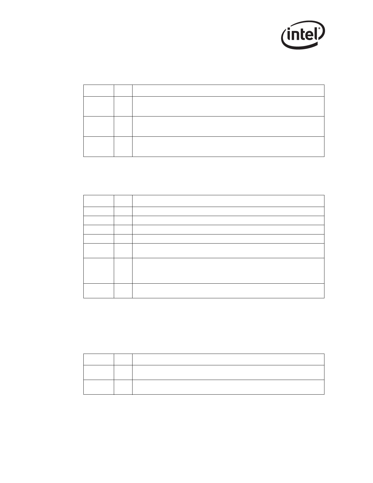
Serializer / Deserializer (SERDES) Signals
3.8
Symbol
RX +/-
TX +/-
SIG_
DETECT
Type
Name and Function
SERDES Receive Pair. These two signals comprise the differential receive pair for the
I
1.25 GHz serial interface. If the SERDES interface is not used, these signals should not
be connected.
SERDES Transmit Pair. These two signals comprise the differential transmit pair for
O
the 1.25 GHz serial interface. If the SERDES interface is not used, these signals should
not be connected.
Signal Detect. This pin indicates when a SERDES signal (connected to the 1.25 GHz
I
serial interface) has been detected by the optical transceiver. If the SERDES interface
is not used, this signal should be connected to ground through a pull-down resistor.
JTAG Test Interface Signals
3.9
3.9.1
Symbol Type
Name and Function
JTAG_TCK I
JTAG_TDI I
JTAG_TDO O
JTAG_TMS I
JTAG_
TRST#
I
CLK_VIEW O
TEST#
I
JTAG Clock.
JTAG TDI.
JTAG TDO.
JTAG TMS.
JTAG Reset. This is an active low reset signal for JTAG. This signal should be
terminated using a pull-down resistor to ground. It must not be left unconnected.
Clock View. The Clock View signal is an output for the clock signals required for IEEE
testing. The clock is selected by register programming. For IEEE testing, a 2-pin header
should be connected to CLK_VIEW with one signal connected to GND, and the other,
to CLK_VIEW.
Factory Test Pin. This is an active low input and has an internal pull-up resistor. For
normal operation, TEST# should be left unconnected.
Power Supply Connections
Power Support Signals
Symbol
CTRL_15
CTRL_25
Type
Name and Function
A
1.5 V Control. The 1.5 V Control signal is an output to an external power transistor. If
regulators are used, it should be left unconnected.
A
2.5 V Control. The 2.5 V Control signal is an output to an external power transistor. If
regulators are used, it should be left unconnected.
16
Datasheet
Share Link: 