HGT1S12N60C3 Просмотр технического описания (PDF) - Harris Semiconductor
Номер в каталоге
Компоненты Описание
производитель
HGT1S12N60C3 Datasheet PDF : 6 Pages
| |||
HGTP12N60C3, HGT1S12N60C3, HGT1S12N60C3S
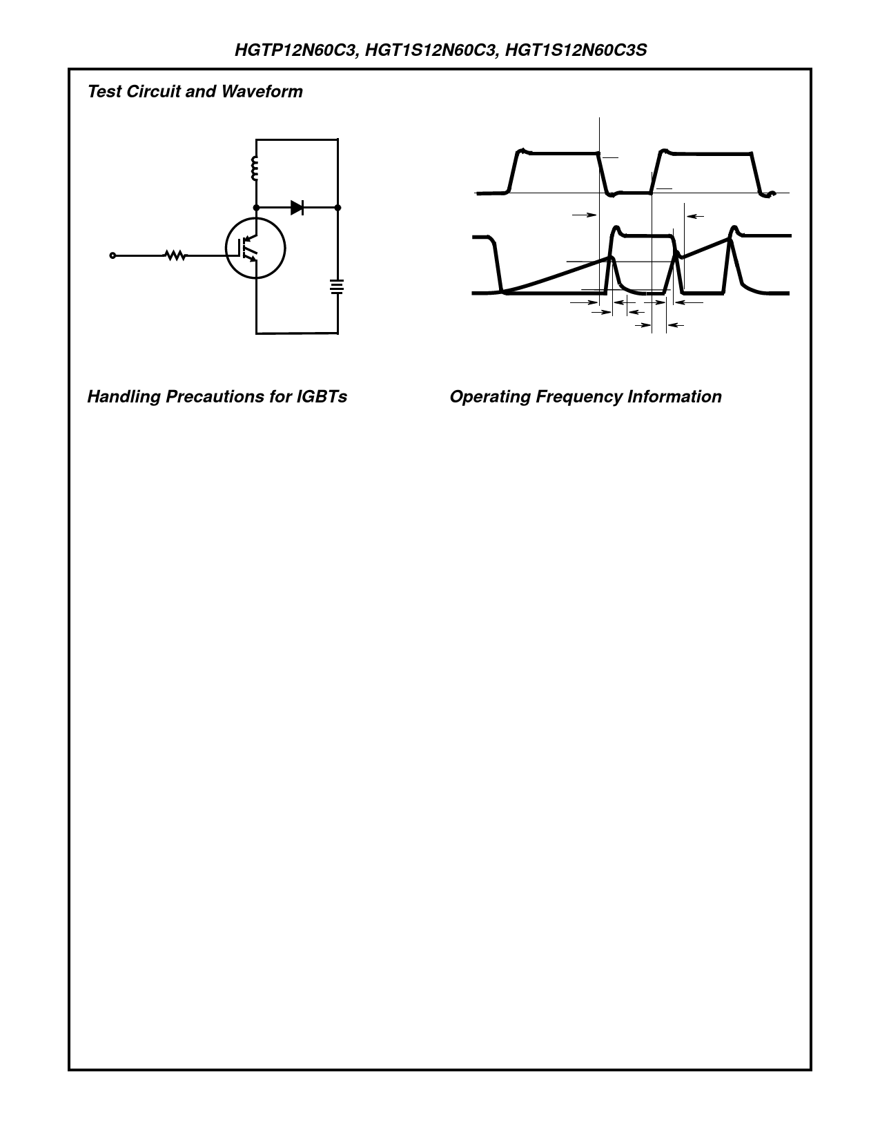
Test Circuit and Waveform
RG = 25Ω
L = 100µH
RHRP1560
+
VDD = 480V
-
FIGURE 18. INDUCTIVE SWITCHING TEST CIRCUIT
90%
VGE
VCE
ICE
10%
EOFF EON
90%
10%
tD(OFF)I tFI
tRI
tD(ON)I
FIGURE 19. SWITCHING TEST WAVEFORMS
Handling Precautions for IGBTs
Operating Frequency Information
Insulated Gate Bipolar Transistors are susceptible to gate-
insulation damage by the electrostatic discharge of energy
through the devices. When handling these devices, care
should be exercised to assure that the static charge built in
the handler’s body capacitance is not discharged through
the device. With proper handling and application procedures,
however, IGBTs are currently being extensively used in pro-
duction by numerous equipment manufacturers in military,
industrial and consumer applications, with virtually no dam-
age problems due to electrostatic discharge. IGBTs can be
handled safely if the following basic precautions are taken:
1. Prior to assembly into a circuit, all leads should be kept
shorted together either by the use of metal shorting
springs or by the insertion into conductive material such
as “ECCOSORBD™ LD26” or equivalent.
2. When devices are removed by hand from their carriers,
the hand being used should be grounded by any suitable
means - for example, with a metallic wristband.
3. Tips of soldering irons should be grounded.
4. Devices should never be inserted into or removed from
circuits with power on.
5. Gate Voltage Rating - Never exceed the gate-voltage rat-
ing of VGEM. Exceeding the rated VGE can result in per-
manent damage to the oxide layer in the gate region.
6. Gate Termination - The gates of these devices are es-
sentially capacitors. Circuits that leave the gate open-cir-
cuited or floating should be avoided. These conditions
can result in turn-on of the device due to voltage buildup
on the input capacitor due to leakage currents or pickup.
Operating frequency information for a typical device
Figure 13) is presented as a guide for estimating device per-
formance for a specific application. Other typical frequency
vs collector current (ICE) plots are possible using the infor-
mation shown for a typical unit in Figures 4, 7, 8, 11 and 12.
The operating frequency plot (Figure 13) of a typical device
shows fMAX1 or fMAX2 whichever is smaller at each point.
The information is based on measurements of a
typical device and is bounded by the maximum rated junc-
tion temperature.
fMAX1 is defined by fMAX1 = 0.05/(tD(OFF)I+ tD(ON)I). Dead-
time (the denominator) has been arbitrarily held to 10% of
the on- state time for a 50% duty factor. Other definitions are
possible. tD(OFF)I and tD(ON)I are defined in Figure 19.
Device turn-off delay can establish an additional frequency
limiting condition for an application other than TJMAX.
tD(OFF)I is important when controlling output ripple under a
lightly loaded condition.
fMAX2 is defined by fMAX2 = (PD - PC)/(EOFF + EON). The
allowable dissipation (PD) is defined by PD = (TJMAX -
TC)/RθJC. The sum of device switching and conduction losses
must not exceed PD. A 50% duty factor was used (Figure 13)
and the conduction losses (PC) are approximated by PC = (VCE
x ICE)/2.
EON and EOFF are defined in the switching waveforms
shown in Figure 19. EON is the integral of the instantaneous
power loss (ICE x VCE) during turn-on and EOFF is the inte-
gral of the instantaneous power loss (ICE x VCE) during turn-
off. All tail losses are included in the calculation for EOFF; i.e.
the collector current equals zero (ICE = 0).
7. Gate Protection - These devices do not have an internal
monolithic zener diode from gate to emitter. If gate pro-
tection is required an external zener is recommended.
ECCOSORBD™ is a Trademark of Emerson and Cumming, Inc.
3-34
Share Link: 