AD9750 –Я—А–Њ—Б–Љ–Њ—В—А —В–µ—Е–љ–Є—З–µ—Б–Ї–Њ–≥–Њ –Њ–њ–Є—Б–∞–љ–Є—П (PDF) - Analog Devices
–Э–Њ–Љ–µ—А –≤ –Ї–∞—В–∞–ї–Њ–≥–µ
–Ъ–Њ–Љ–њ–Њ–љ–µ–љ—В—Л –Ю–њ–Є—Б–∞–љ–Є–µ
–њ—А–Њ–Є–Ј–≤–Њ–і–Є—В–µ–ї—М
AD9750 Datasheet PDF : 22 Pages
| |||

AD9750
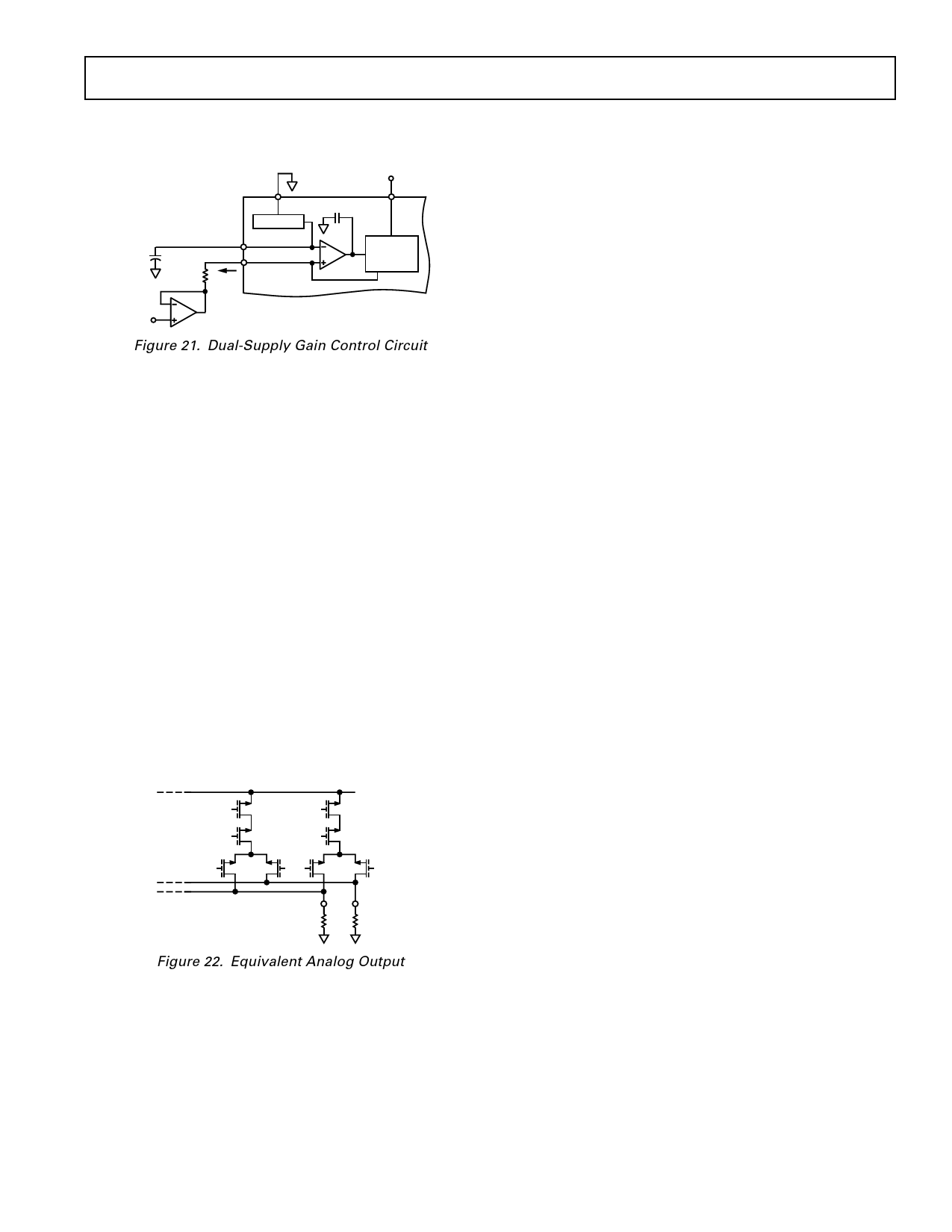
and 625 µA, respectively. The associated equations in Figure 21
can be used to determine the value of RSET.
AVDD
REFLO 150pF
+1.2V REF
AVDD
REFIO
1вРЃF
FS ADJ
RSET IREF
AD9750
CURRENT
SOURCE
ARRAY
VGC
IREF = (1.2вАУVGC)/RSET
WITH VGC < VREFIO AND 62.5вРЃA ’Е IREF ’Е 625A
Figure 21. Dual-Supply Gain Control Circuit
ANALOG OUTPUTS
The AD9750 produces two complementary current outputs,
IOUTA and IOUTB, which may be configured for single-end
or differential operation. IOUTA and IOUTB can be converted
into complementary single-ended voltage outputs, VOUTA and
VOUTB, via a load resistor, RLOAD, as described in the DAC
Transfer Function section by Equations 5 through 8. The
differential voltage, VDIFF, existing between VOUTA and VOUTB
can also be converted to a single-ended voltage via a transformer
or differential amplifier configuration.
Figure 22 shows the equivalent analog output circuit of the
AD9750 consisting of a parallel combination of PMOS differen-
tial current switches associated with each segmented current
source. The output impedance of IOUTA and IOUTB is deter-
mined by the equivalent parallel combination of the PMOS
switches and is typically 100 kвД¶ in parallel with 5 pF. Due to
the nature of a PMOS device, the output impedance is also
slightly dependent on the output voltage (i.e., VOUTA and VOUTB)
and, to a lesser extent, the analog supply voltage, AVDD, and
full-scale current, IOUTFS. Although the output impedanceвАЩs
signal dependency can be a source of dc nonlinearity and ac linear-
ity (i.e., distortion), its effects can be limited if certain precau-
tions are noted.
AVDD
IOUTA
RLOAD
IOUTB
RLOAD
Figure 22. Equivalent Analog Output
IOUTA and IOUTB also have a negative and positive voltage
compliance range. The negative output compliance range of
вАУ1.0 V is set by the breakdown limits of the CMOS process.
Operation beyond this maximum limit may result in a break-
down of the output stage and affect the reliability of the AD9750.
The positive output compliance range is slightly dependent on
the full-scale output current, IOUTFS. It degrades slightly from its
nominal 1.25 V for an IOUTFS = 20 mA to 1.00 V for an IOUTFS =
2 mA. Operation beyond the positive compliance range will
induce clipping of the output signal which severely degrades
the AD9750вАЩs linearity and distortion performance.
For applications requiring the optimum dc linearity, IOUTA
and/or IOUTB should be maintained at a virtual ground via an
I-V op amp configuration. Maintaining IOUTA and/or IOUTB
at a virtual ground keeps the output impedance of the AD9750
fixed, significantly reducing its effect on linearity. However,
it does not necessarily lead to the optimum distortion perfor-
mance due to limitations of the I-V op amp. Note that the
INL/DNL specifications for the AD9750 are measured in
this manner using IOUTA. In addition, these dc linearity
specifications remain virtually unaffected over the specified
power supply range of 4.5 V to 5.5 V.
Operating the AD9750 with reduced voltage output swings at
IOUTA and IOUTB in a differential or single-ended output
configuration reduces the signal dependency of its output
impedance thus enhancing distortion performance. Although
the voltage compliance range of IOUTA and IOUTB extends
from вАУ1.0 V to +1.25 V, optimum distortion performance is
achieved when the maximum full-scale signal at IOUTA and
IOUTB does not exceed approximately 0.5 V. A properly se-
lected transformer with a grounded center-tap will allow the
AD9750 to provide the required power and voltage levels to
different loads while maintaining reduced voltage swings at
IOUTA and IOUTB. DC-coupled applications requiring a
differential or single-ended output configuration should size
RLOAD accordingly. Refer to Applying the AD9750 section for
examples of various output configurations.
The most significant improvement in the AD9750вАЩs distortion
and noise performance is realized using a differential output
configuration. The common-mode error sources of both IOUTA
and IOUTB can be substantially reduced by the common-mode
rejection of a transformer or differential amplifier. These
common-mode error sources include even-order distortion
products and noise. The enhancement in distortion performance
becomes more significant as the reconstructed wave-formвАЩs
frequency content increases and/or its amplitude decreases.
The distortion and noise performance of the AD9750 is also
slightly dependent on the analog and digital supply as well as the
full-scale current setting, IOUTFS. Operating the analog supply at
5.0 V ensures maximum headroom for its internal PMOS current
sources and differential switches leading to improved distortion
performance. Although IOUTFS can be set between 2 mA and
20 mA, selecting an IOUTFS of 20 mA will provide the best dis-
tortion and noise performance also shown in Figure 8. The
noise performance of the AD9750 is affected by the digital sup-
ply (DVDD), output frequency, and increases with increasing
clock rate as shown in Figure 11. Operating the AD9750 with
low voltage logic levels between 3 V and 3.3 V will slightly re-
duce the amount of on-chip digital noise.
In summary, the AD9750 achieves the optimum distortion and
noise performance under the following conditions:
(1) Differential Operation.
(2) Positive voltage swing at IOUTA and IOUTB limited to
+0.5 V.
(3) IOUTFS set to 20 mA.
(4) Analog Supply (AVDD) set at 5.0 V.
(5) Digital Supply (DVDD) set at 3.0 V to 3.3 V with appro-
priate logic levels.
Note that the ac performance of the AD9750 is characterized
under the above mentioned operating conditions.
REV. 0
вАУ11вАУ