LQFP100 Просмотр технического описания (PDF) - NXP Semiconductors.
Номер в каталоге
Компоненты Описание
производитель
LQFP100 Datasheet PDF : 69 Pages
| |||
NXP Semiconductors
LPC2364/65/66/67/68
Single-chip 16-bit/32-bit microcontrollers
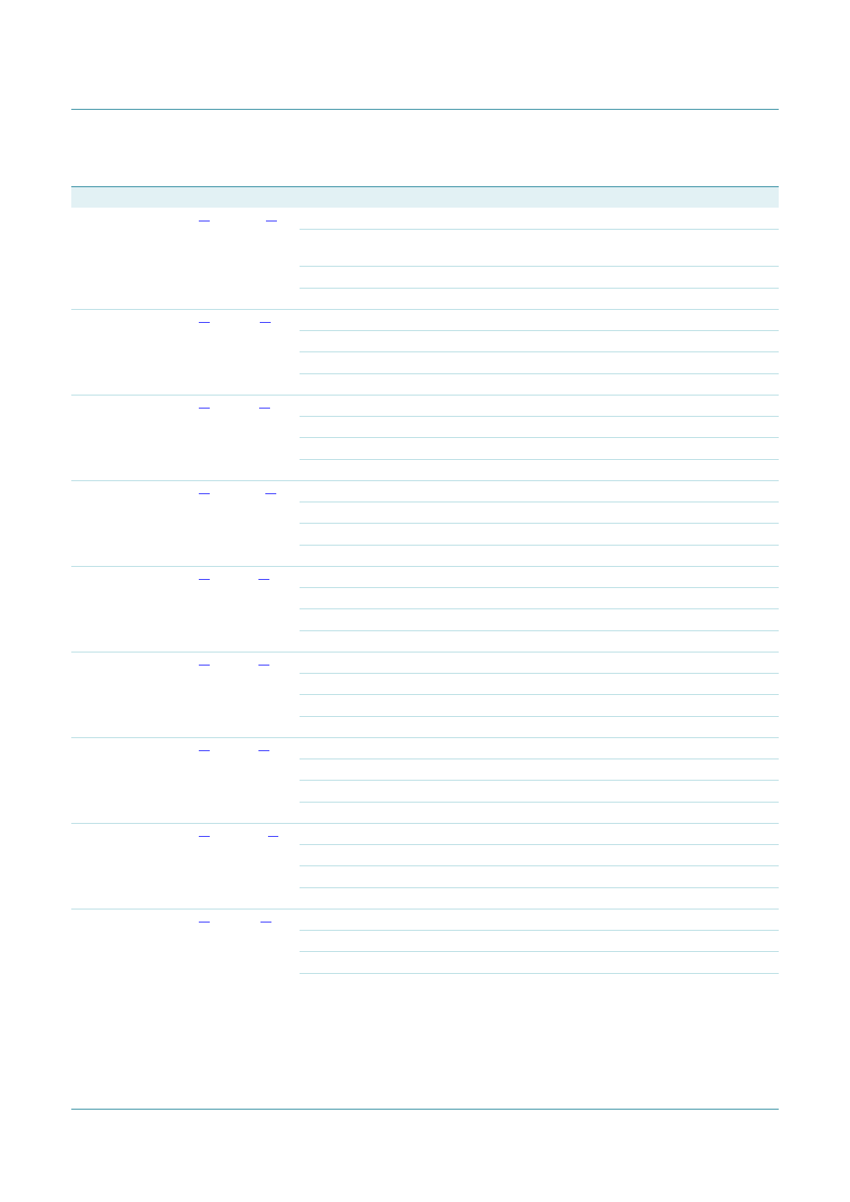
Table 4. Pin description …continued
Symbol
Pin
Ball
Type
P0[9]/
76[1]
I2STX_SDA/
MOSI1/MAT2[3]
A10[1] I/O
I/O
P0[10]/TXD2/
48[1]
SDA2/MAT3[0]
P0[11]/RXD2/
49[1]
SCL2/MAT3[1]
P0[15]/TXD1/
SCK0/SCK
62[1]
P0[16]/RXD1/
SSEL0/SSEL
63[1]
P0[17]/CTS1/
MISO0/MISO
61[1]
P0[18]/DCD1/
MOSI0/MOSI
60[1]
P0[19]/DSR1/
MCICLK/SDA1
59[1]
P0[20]/DTR1/
58[1]
MCICMD/SCL1
I/O
O
H7[1]
I/O
O
I/O
O
K9[1]
I/O
I
I/O
O
F10[1] I/O
O
I/O
I/O
F8[1]
I/O
I
I/O
I/O
F9[1]
I/O
I
I/O
I/O
F6[1]
I/O
I
I/O
I/O
G10[1] I/O
I
O
I/O
G9[1]
I/O
O
I
I/O
Description
P0[9] — General purpose digital input/output pin.
I2STX_SDA — Transmit data. It is driven by the transmitter and read by the
receiver. Corresponds to the signal SD in the I2S-bus specification.
MOSI1 — Master Out Slave In for SSP1.
MAT2[3] — Match output for Timer 2, channel 3.
P0[10] — General purpose digital input/output pin.
TXD2 — Transmitter output for UART2.
SDA2 — I2C2 data input/output (this is not an open-drain pin).
MAT3[0] — Match output for Timer 3, channel 0.
P0[11] — General purpose digital input/output pin.
RXD2 — Receiver input for UART2.
SCL2 — I2C2 clock input/output (this is not an open-drain pin).
MAT3[1] — Match output for Timer 3, channel 1.
P0[15] — General purpose digital input/output pin.
TXD1 — Transmitter output for UART1.
SCK0 — Serial clock for SSP0.
SCK — Serial clock for SPI.
P0[16] — General purpose digital input/output pin.
RXD1 — Receiver input for UART1.
SSEL0 — Slave Select for SSP0.
SSEL — Slave Select for SPI.
P0[17] — General purpose digital input/output pin.
CTS1 — Clear to Send input for UART1.
MISO0 — Master In Slave Out for SSP0.
MISO — Master In Slave Out for SPI.
P0[18] — General purpose digital input/output pin.
DCD1 — Data Carrier Detect input for UART1.
MOSI0 — Master Out Slave In for SSP0.
MOSI — Master Out Slave In for SPI.
P0[19] — General purpose digital input/output pin.
DSR1 — Data Set Ready input for UART1.
MCICLK — Clock output line for SD/MMC interface. (LPC2367/68 only)
SDA1 — I2C1 data input/output (this is not an open-drain pin).
P0[20] — General purpose digital input/output pin.
DTR1 — Data Terminal Ready output for UART1.
MCICMD — Command line for SD/MMC interface. (LPC2367/68 only)
SCL1 — I2C1 clock input/output (this is not an open-drain pin).
LPC2364_65_66_67_68
Product data sheet
All information provided in this document is subject to legal disclaimers.
Rev. 7.1 — 16 October 2013
© NXP B.V. 2013. All rights reserved.
11 of 69
Share Link: 