LC651154F Просмотр технического описания (PDF) - SANYO -> Panasonic
Номер в каталоге
Компоненты Описание
производитель
LC651154F Datasheet PDF : 39 Pages
| |||
LC651154N, 651154F, 651154L, 651152N, 651152F, 651152L
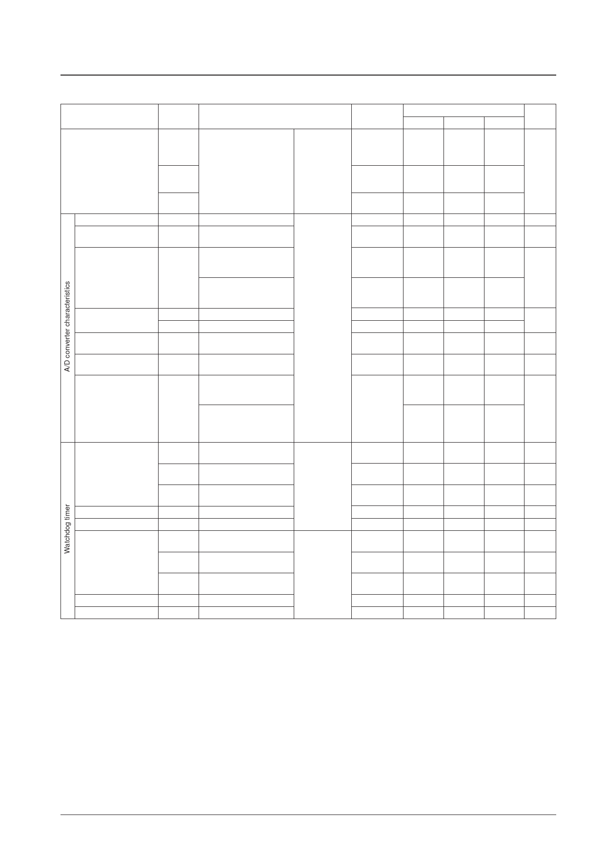
Continued from preceding page.
Parameter
Symbol
Conditions
Applicable pins
Ratings
Unit
and notes
min
typ
max
Pulse output function
• Figure 7
Period
tPCY
• TCYC = 4 × system clock
PE0
period
• With an external resistor of
High-level pulse width
tPH
1 kΩ and an external
PE0
capacitor of 50 pF on only
the n-channel open-drain
Low-level pulse width
tPL
pins.
PE0
64 × TCYC
32 × TCYC
±10%
µs
32 × TCYC
±10%
Resolution
8
bit
Absolute precision
Conversion time
Input reference voltage
Input reference current
range
TCAD
AV+
AV–
IRIF
AV+ = VDD
AV– = VSS
When the A/D converter
speed is normal (1:1),
namely 26 × TCYC
When the A/D converter
speed is one half (1:2),
namely 51 × TCYC
AV+ = VDD, AV– = VSS
AV+
VDD = 3 to 6 V AV–
AV+, AV–
72
(TCYC =
2.77 µs)
141
(TCYC =
2.77 µs)
AV–
VSS
200
±1
±2 LSB
312
(TCYC =
12 µs)
µs
612
(TCYC =
12 µs)
VDD
V
AV+
500
800 µA
Analog input voltage
range
VAIN
AD0 to AD7
AV–
AV+ V
Including the output off
leakage current.
VAIN = VDD
Analog port input current
IAIN
VAIN = VSS
AD0 to AD7
(The I/O
shared
function ports
have open-
drain
–1
specifications.)
1
µA
Cw
When PE1 has the
open-drain specifications.
WDR
0.1 ±5%
µF
Recommended
constants*10
Rw
When PE1 has the
open-drain specifications.
WDR
RI
When PE1 has the
VDD = 3 to 6 V
WDR
open-drain specifications.
680 ±1%
kΩ
100 ±1%
Ω
Clear time (discharge)
Clear period (charge)
tWCT
tWCCY
Cw
Figure 8
Figure 8
When PE1 has the
open-drain specifications.
WDR
100
µs
WDR
36
ms
WDR
0.047 ±5%
µF
Recommended
constants*10
Rw
When PE1 has the
open-drain specifications.
WDR
RI
When PE1 has the
VDD = 3 to 6 V
WDR
open-drain specifications.
680 ±1%
kΩ
100 ±1%
Ω
Clear time (discharge)
Clear period (charge)
tWCT
tWCCY
Figure 8
Figure 8
WDR
40
µs
WDR
18
ms
Notes:1. Allowed up to the amplitude generated when the oscillator shown in figure 3 is used with the recommended circuit constants and driven by the IC.
2. The average over a 100 ms period.
3. The operating VDD supply voltage must be maintained from the point the HALT instruction is executed until the IC has fully entered the standby
state. Applications must also assure that no chattering occurs on the PA3 pin during the HALT instruction execution cycle.
4. Recommended circuit constants that have been verified to oscillate stably according to the oscillator element manufacturer using the Sanyo-
stipulated oscillator characteristics evaluation board.
5. The OSC1 pin will have Schmitt characteristics when external clock oscillator is selected with the two-pin RC oscillator option.
6. These are the results of testing using our (Sanyo’s) characteristics evaluation board with the recommended circuit constants used as external
components. The current flowing in the IC’s output transistors and transistors that have pull-up resistors is not included.
7. fCFOSC is the frequency when the recommended circuit constants from table 1 are used as external components.
8. Indicates the time required to achieve stable oscillation from the point VDD rises above the lower limit of the operating voltage range.
9. TCYC = 4 × the system clock period
10. If the application could be used in an environment in which condensation is possible, extra care with respect to the leakage between PE1 and
adjacent pins and leakage associated with external resistors and capacitor is required during design.
No. 6278-16/39
Share Link: 