LC651154F Просмотр технического описания (PDF) - SANYO -> Panasonic
Номер в каталоге
Компоненты Описание
производитель
LC651154F Datasheet PDF : 39 Pages
| |||
LC651154N, 651154F, 651154L, 651152N, 651152F, 651152L
LC651154N, 651152N
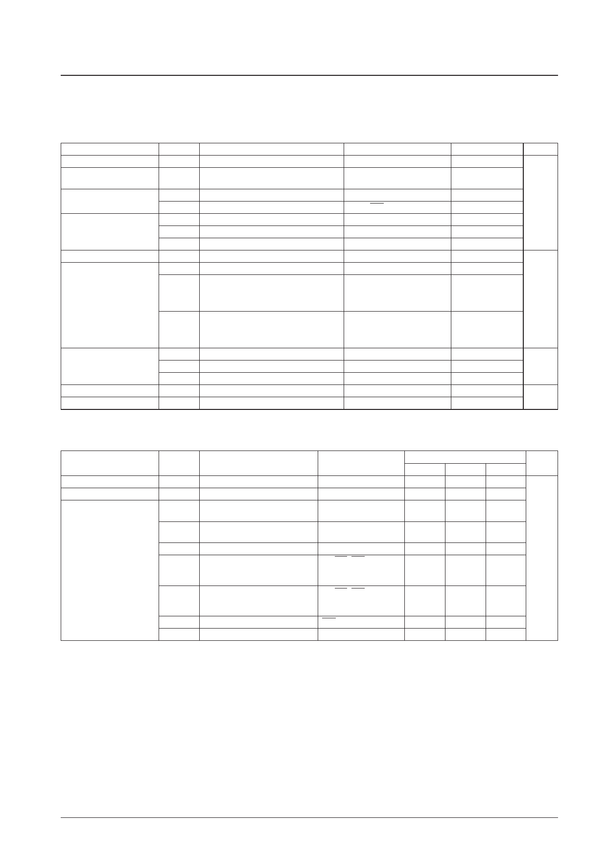
Absolute Maximum Ratings at Ta = 25°C, VSS = 0 V
Parameter
Symbol
Conditions
Applicable pins and notes
Ratings
Unit
Maximum supply voltage
Output voltage
VDD max
VO
VDD
OSC2
–0.3 to +7.0
Allowed up to the
generated voltage.
Input voltage
I/O voltage
Peak output current
Average output current
VI (1)
VI (2)
VIO (1)
VIO (2)
VIO (3)
IOP
IOA
PC0 to 3, PD0 to 3, PE0, 1, PF0 to 3
PC0 to 3, PD0 to 3, PE0, 1, PF0 to 3
PC0 to 3, PG0 to 3
Per single pin, averaged over 100 ms
∑IOA (1)
The total current for PC0 to PC3,
PD0 to PD3, and PE0 to PE1 *2
OSC1 *1
TEST, RES, AV+, AV–
–0.3 to VDD + 0.3
V
–0.3 to VDD + 0.3
Open-drain specification ports
–0.3 to +15
Pull-up resistor specification ports
I/O ports
–0.3 to VDD + 0.3
–0.3 to VDD + 0.3
–2 to +20
I/O ports
–2 to +20
PC0 to 3
PD0 to 3
PE0 to 1
–15 to +100
mA
∑IOA (2)
The total current for PF0 to PF3,
PG0 to PG3, and PA0 to PA3 (See note 2.) *2
PF0 to 3
PG0 to 3
PA0 to 3
–15 to +100
Pd max (1) Ta = –40 to +85°C (DIP package)
310
Allowable power dissipation Pd max (2) Ta = –40 to +85°C (MFP package)
220
mW
Pd max (3) Ta = –40 to +85°C (SSOP package)
160
Operating temperature
Storage temperature
Topr
Tstg
–40 to +85
°C
–55 to +125
Allowable Operating Ranges at Ta = –40 to +85°C, VSS = 0 V, VDD = 3.0 to 6.0 V (Unless otherwise specified.)
Parameter
Operating supply voltage
Standby supply voltage
High-level input voltage
Symbol
VDD
VST
VIH (1)
VIH (2)
VIH (3)
VIH (4)
VIH (5)
VIH (6)
VIH (7)
Conditions
Applicable pins and notes
VDD
RAM and register values retained*3 VDD
Output n-channel transistors off
Ports C, D, E, and F with
open-drain specifications
Output n-channel transistors off
Ports C, D, E, and F with
pull-up resistor specifications
Output n-channel transistors off
Port A, G
Output n-channel transistors off
The INT, SCK, and SI
pins with open-drain
specifications
Output n-channel transistors off
The INT, SCK, and SI
pins with pull-up resistor
specifications
VDD = 1.8 to 6.0 V
External clock specifications
RES
OSC1
min
3.0
1.8
0.7 VDD
0.7 VDD
0.7 VDD
0.8 VDD
0.8 VDD
0.8 VDD
0.8 VDD
Ratings
typ
Unit
max
6.0
6.0
13.5
VDD
VDD
V
13.5
VDD
VDD
VDD
Continued on next page.
No. 6278-12/39
Share Link: 