LC651154F Просмотр технического описания (PDF) - SANYO -> Panasonic
Номер в каталоге
Компоненты Описание
производитель
LC651154F Datasheet PDF : 39 Pages
| |||
LC651154N, 651154F, 651154L, 651152N, 651152F, 651152L
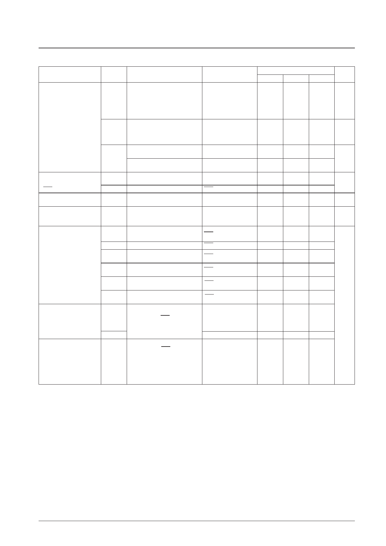
Continued from preceding page.
Parameter
Symbol
Conditions
Applicable pins and notes
Oscillator characteristics
Ceramic oscillator
Oscillator frequency
Oscillator stabilization time
(note 8)
Two-pin RC oscillator
Oscillator frequency
Pull-up resistor
I/O ports
RES
External reset characteristics
Reset time
Pin capacitances
Serial clock
Input clock cycle time
Output clock cycle time
Input clock low-level pulse
width
Output clock low-level pulse
width
Input clock high-level pulse
width
Output clock high-level
pulse width
Serial input
Data setup time
fCFOSC*7
tCFS
fMOSC
RPP
Ru
tRST
Cp
tCKCY (1)
tCKCY (2)
tCKL (1)
tCKL (2)
tCKH (1)
tCKH (2)
tICK
• Figure 3, fo = 400 kHz
• Figure 3, fo = 800 kHz
• Figure 3, fo = 1 MHz
• Figure 3, fo = 4 MHz, with the
divide-by-three or divide-by-four
circuit used.
• Figure 4, fo = 400 kHz
• Figure 4, fo = 800 kHz, 1 MHz, or
4 MHz, with the divide-by-three or
divide-by-four circuit used.
• Figure 2, Cext = 270 pF ±5%
• Figure 2, Rext = 5.6 kΩ ±1%
• Figure 2, Cext = 270 pF ±5%
• Figure 2, Rext = 12 kΩ ±1%
• Output n-channel transistors off
• VIN = VSS, VDD = 5 V
VIN = VSS, VDD = 5 V
• f = 1 MHz
• With all pins other than the pin
being tested at VIN = VSS.
Figure 6
Figure 6
Figure 6
Figure 6
Figure 6
Figure 6
• Stipulated with respect to the
rising edge of SCK.
• Figure 6
OSC1, OSC2
OSC1, OSC2
OSC1, OSC2
OSC1, OSC2
OSC1, OSC2
OSC1, OSC2
Pull-up resistor
specification ports
RES
SCK
SCK
SCK
SCK
SCK
SCK
SI
Data hold time
Serial output
Output delay time
tCKI
tCKO
SI
• Stipulated with respect to the
falling edge of SCK.
• With an external resistor of 1 kΩ
and an external capacitor of 50 pF SO
on only the n-channel open-drain
pins.
• Figure 6
min
392
784
980
3920
Ratings
typ
400
800
1000
4000
Unit
max
408
816
1020 kHz
4080
10
10
ms
587
800
290
400
8
14
200
500
See figure 5.
10
2.0
64 × TCYC*9
1.0
32 × TCYC
1.0
32 × TCYC
0.4
1298
kHz
818
30
kΩ
800
pF
µs
0.4
0.6
Continued on next page.
No. 6278-15/39
Share Link: 