HMS30C7202N Просмотр технического описания (PDF) - MagnaChip Semiconductor
Номер в каталоге
Компоненты Описание
производитель
HMS30C7202N Datasheet PDF : 179 Pages
| |||
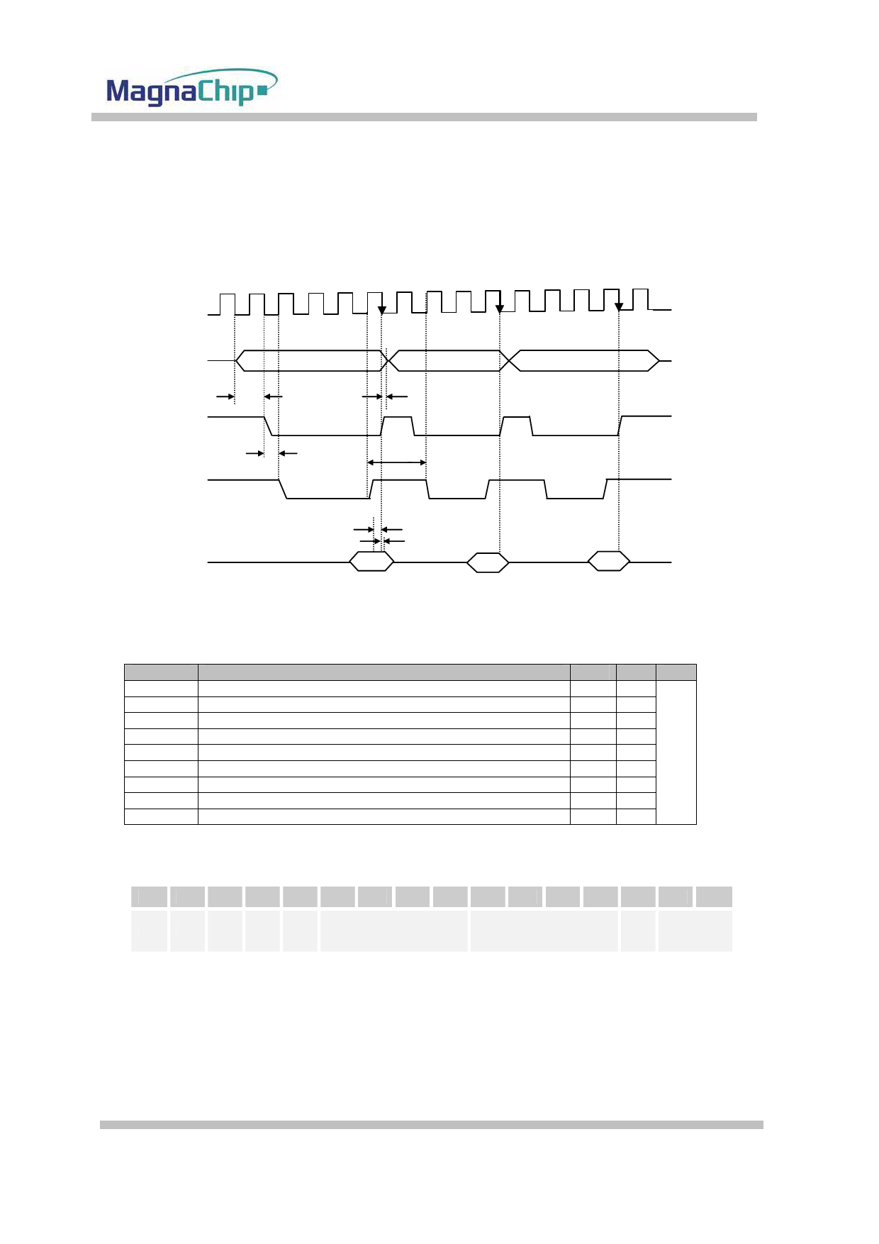
12.5 AC Characteristics
12.5.1 Static Memory Interface
12.5.1.1 READ Access Timing (Single Mode)
BCLK
RA
nRCS
nROE
tSU(A)
tSU(CE0)
RD
A
B
tHO(A)
tREC
tSU(D)
tHO(D)
HMS30C7202N
C
Symbol
Parameter
Min Max Unit
tSU(A)
Address to nRCS falling-edge setup time
25
tHO(A)
nROE rising-edge to Address hold time
0
tSU(CE0)
nRCS falling-edge to nROE falling-edge setup time
13
tHO(CE0)
nROE rising-edge to nRCS rising-edge setup time
-13
tHO(CE1) nROE or nRWE rising-edge to nRCS falling-edge hold time 15
ns
tSU(CE1) nRCS rising-edge to nROE or nRWE falling-edge setup time 25
tREC
nROE negate to start of next cycle
50
tSU(D)
Data setup time before latch
5
tHO(D)
Data hold time after latch
0
Timing values for read access in single mode data transfer
Memory Configuration Register Setting = 0x060
11 10 9
8
7
0
0 0 00
6
5
4
3
1 10 0
2
1
0
0
00
© 2004 MagnaChip Semiconductor Ltd. All R1ig65hts Reserved.
- 165 -
Version 1.1
Share Link: 