LTC1325CN Просмотр технического описания (PDF) - Linear Technology
Номер в каталоге
Компоненты Описание
производитель
LTC1325CN Datasheet PDF : 24 Pages
| |||
LTC1325
FUNCTIONAL DESCRIPTIO
Bit 13: Power Shutdown (PS)
PS selects between the normal operating mode, or the
shutdown mode.
PS
DESCRIPTION
0
Normal Operation
1
Shutdown All Circuits Except Digital Inputs
Bits 14 to 16: Duty Ratio Select (DR0 to DR2)
DR2, DR1 and DR0 select the duty cycle of the charging
loop operation (not 111kHz PWM duty cycle). The last
three selections place the chip into a test mode and should
not be used.
DR2 DR1 DR0 DESCRIPTION
0
0
0 1/16
0
0
1 1/8
0
1
0 1/4
0
1
1 1/2
1
0
01
1
0
1 Test Mode 1
1
1
0 Test Mode 2
1
1
1 Test Mode 3
Bits 21 and 22: Charging Loop Reference Voltage
Select (VR0 and VR1)
VR1 and VR0 select the desired reference voltage VCHRG
for the charging loop. The charging loop will force the
average voltage at the Sense pin to be equal to VDAC. The
average charging current is VDAC/RSENSE (see Figure 4).
VR1
VR0
VDAC (mV)
0
0
18
0
1
34
1
0
55
1
1
160
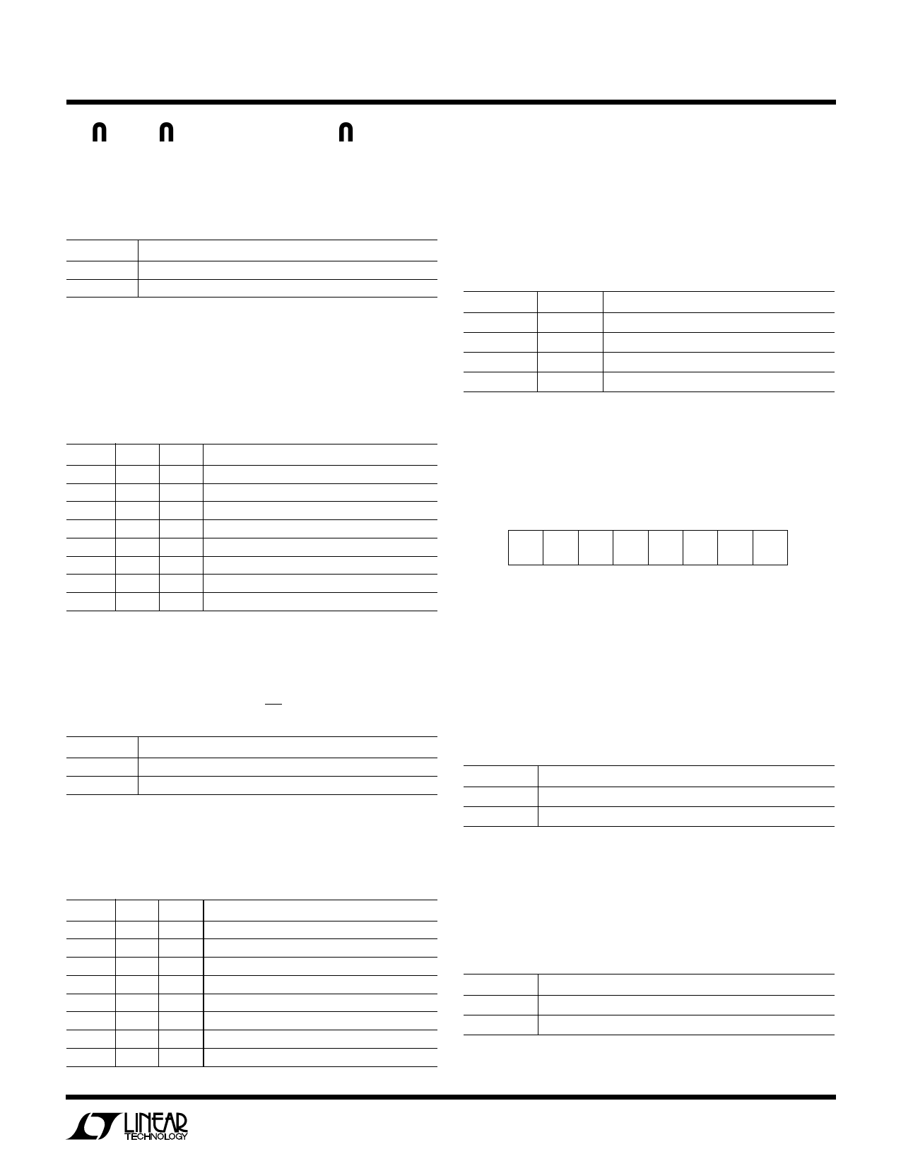
STATUS WORD
The status word is 8 bits long and contains the status of
the internal fail-safe circuits.
1
2
3
4
5
6
7
8
BATP BATR FMCV FEDV FHTF FLTF tOUT FS
LTC1325 • F02
Figure 2. Status Word
Bit 17: Fail-Safe Latch Clear (FSCLR)
When FSCLR bit is set to one, the internal fail-safe timer is
reset to 0, and the fail-safe latches are reset. FSCLR is
automatically reset to 0 when CS goes high.
FSCLR
0
1
DESCRIPTION
No Action
Reset Fail-Safe Timer and Latches
Bits 18 to 20: Timeout Period Select (TO0 to TO2)
TO2, TO1 and TO0 select the desired fail-safe timeout
period,tOUT. On power-up, the default timeout is 5 minutes.
TO2 TO1 TO0 TIMEOUT (MINUTES)
0
0
05
0
0
1 10
0
1
0 20
0
1
1 40
1
0
0 80
1
0
1 160
1
1
0 320
1
1
1 Indefinite (No Timeout)
Bit 1: Battery Present (BATP)
The BATP bit = 1 indicates the presence of the battery. The
bit is set to 1 when the voltage at the VBAT pin falls below
(VDD – 1.8V). BATP = 0 when the battery is removed and
VBAT is pulled high by RTRK (see Figure 3).
BATP
0
1
CONDITIONS
(VDD – 1.8) < VBAT < VDD
VBAT < (VDD – 1.8)
Bit 2: Battery Reversed (BATR) or Shorted
The BATR bit indicates when the battery is connected
backwards or shorted. The bit is set when the battery cell
voltage at the output of the battery divider VCELL is below
100mV.
BATR
0
1
CONDITIONS
VCELL > 100mV
VCELL < 100mV
11
Share Link: 