EV-ADF4196SD1Z Просмотр технического описания (PDF) - Analog Devices
Номер в каталоге
Компоненты Описание
производитель
EV-ADF4196SD1Z Datasheet PDF : 28 Pages
| |||
Data Sheet
ADF4196
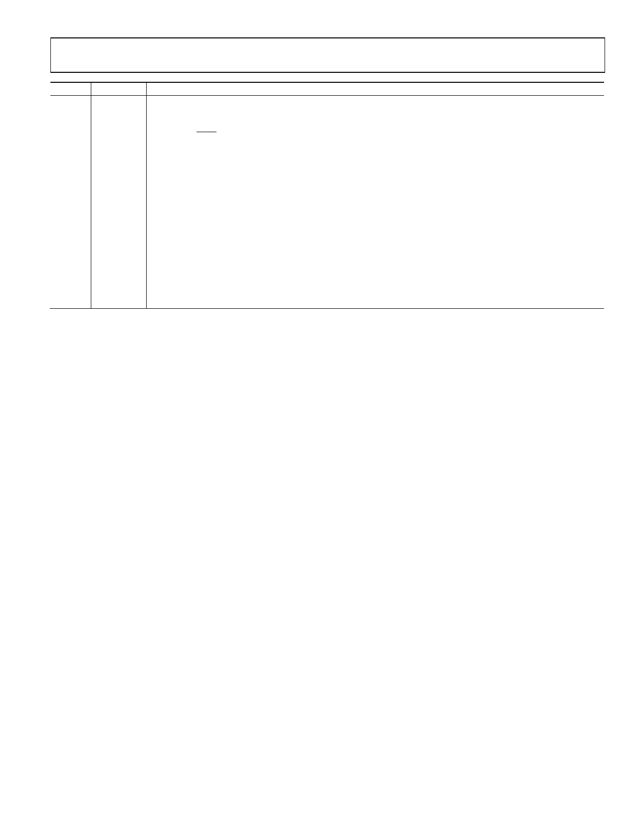
Pin No.
23
24
25
26
27
28
29
30
31
32
Mnemonic
RSET
VP2
AIN−
CPOUT−
SW2
SWGND
SW1
CPOUT+
AIN+
VP3
EP
Description
Connecting a resistor between this pin and GND sets the charge pump output current. The nominal voltage bias at
the RSET pin is 0.55 V. The relationship between ICP and RSET is
ICP
=
0.25
RSET
Therefore, with RSET = 2.4 kΩ, ICP = 104 µA.
Power Supply Pin for the Charge Pump. Nominally 5 V, VP2 should be at the same voltage as VP1. Place a 0.1 µF
decoupling capacitor to the ground plane as close as possible to this pin.
Negative Input Pin for the Differential Amplifier.
Differential Charge Pump Negative Output Pin. Connect this pin to AIN− and the loop filter.
Fast Lock Switch 2. This switch is closed to SWGND when the SW1/SW2 timeout counter is active.
Ground for SW1 and SW2 Switches. Connect this pin to the ground plane.
Fast Lock Switch 1. This switch is closed to SWGND when the SW1/SW2 timeout counter is active.
Differential Charge Pump Positive Output Pin. Connect this pin to AIN+ and the loop filter.
Positive Input Pin for the Differential Amplifier.
Power Supply Pin for the Differential Amplifier. Ranges from 5.0 V to 5.5 V. Place a 0.1 µF decoupling capacitor to
the ground plane as close as possible to this pin. VP3 also requires a 10 µF decoupling capacitor to the ground plane.
Exposed Paddle. The exposed paddle must be connected to the ground plane.
Rev. D | Page 7 of 28
Share Link: 