AD9767-EB –ü—Ä–æ—Å–º–æ—Ç—Ä —Ç–µ—Ö–Ω–∏—á–µ—Å–∫–æ–≥–æ –æ–ø–∏—Å–∞–Ω–∏—è (PDF) - Analog Devices
–ù–æ–º–µ—Ä –≤ –∫–∞—Ç–∞–ª–æ–≥–µ
–ö–æ–º–ø–æ–Ω–µ–Ω—Ç—ã –û–ø–∏—Å–∞–Ω–∏–µ
–ø—Ä–æ–∏–∑–≤–æ–¥–∏—Ç–µ–ª—å
AD9767-EB Datasheet PDF : 27 Pages
| |||
AD9767
Performing a differential-to-single-ended conversion via a trans-
former also provides the ability to deliver twice the reconstructed
signal power to the load (i.e., assuming no source termination).
Since the output currents of IOUTA and IOUTB are complemen-
tary, they become additive when processed differentially. A
properly selected transformer will allow the AD9767 to provide
the required power and voltage levels to different loads.
The output impedance of IOUTA and IOUTB is determined by the
equivalent parallel combination of the PMOS switches associ-
ated with the current sources and is typically 100 kΩ in parallel
with 5 pF. It is also slightly dependent on the output voltage
(i.e., VOUTA and VOUTB) due to the nature of a PMOS device.
As a result, maintaining IOUTA and/or IOUTB at a virtual ground
via an I-V op amp configuration will result in the optimum dc
linearity. Note the INL/DNL specifications for the AD9767
are measured with IOUTA maintained at a virtual ground via an
op amp.
IOUTA and IOUTB also have a negative and positive voltage com-
pliance range that must be adhered to in order to achieve opti-
mum performance. The negative output compliance range of
–1.0 V is set by the breakdown limits of the CMOS process.
Operation beyond this maximum limit may result in a break-
down of the output stage and affect the reliability of the AD9767.
The positive output compliance range is slightly dependent on
the full-scale output current, IOUTFS. It degrades slightly from
its nominal 1.25 V for an IOUTFS = 20 mA to 1.00 V for an
IOUTFS = 2 mA. The optimum distortion performance for a
single-ended or differential output is achieved when the maxi-
mum full-scale signal at IOUTA and IOUTB does not exceed 0.5 V.
Applications requiring the AD9767’s output (i.e., VOUTA and/or
VOUTB) to extend its output compliance range should size RLOAD
accordingly. Operation beyond this compliance range will ad-
versely affect the AD9767’s linearity performance and subse-
quently degrade its distortion performance.
DIGITAL INPUTS
The AD9767’s digital inputs consist of two channels. For the
dual port mode, each DAC has its own dedicated 14-bit data
port, WRT line and CLK line. In the interleaved timing mode,
the function of the digital control pins changes as described in
the Interleaved Mode Timing section. The 14-bit parallel data
inputs follow straight binary coding where DB13 is the Most
Significant Bit (MSB) and DB0 is the Least Significant Bit
(LSB). IOUTA produces a full-scale output current when all data
bits are at Logic 1. IOUTB produces a complementary output
with the full-scale current split between the two outputs as a
function of the input code.
The digital interface is implemented using an edge-triggered
master slave latch. The DAC outputs are updated following
either the rising edge, or every other rising edge of the clock,
depending on whether dual or interleaved mode is being used.
The DAC outputs are designed to support a clock rate as high
as 125 MSPS. The clock can be operated at any duty cycle that
meets the specified latch pulsewidth. The setup and hold times
can also be varied within the clock cycle as long as the specified
minimum times are met, although the location of these transi-
tion edges may affect digital feedthrough and distortion perfor-
mance. Best performance is typically achieved when the input
data transitions on the falling edge of a 50% duty cycle clock.
DAC TIMING
The AD9767 can operate in two timing modes, dual and inter-
leaved, which are described below. The block diagram in Figure
25 represents the latch architecture in the interleaved timing mode.
DUAL PORT MODE TIMING
For the following section, refer to Figure 2.
When the mode pin is at Logic 1, the AD9767 operates in dual
port mode. The AD9767 functions as two distinct DACs. Each
DAC has its own completely independent digital input and
control lines.
The AD9767 features a double buffered data path. Data enters
the device through the channel input latches. This data is then
transferred to the DAC latch in each signal path. Once the data
is loaded into the DAC latch, the analog output will settle to its
new value.
For general consideration, the WRT lines control the channel
input latches and the CLK lines control the DAC latches. Both
sets of latches are updated on the rising edge of their respective
control signals.
The rising edge of CLK should occur before or simultaneously
with the rising edge of WRT. Should the rising edge of CLK
occur after the rising edge of WRT, a 2 ns minimum delay should
be maintained from the rising edge of WRT to the rising edge of
CLK.
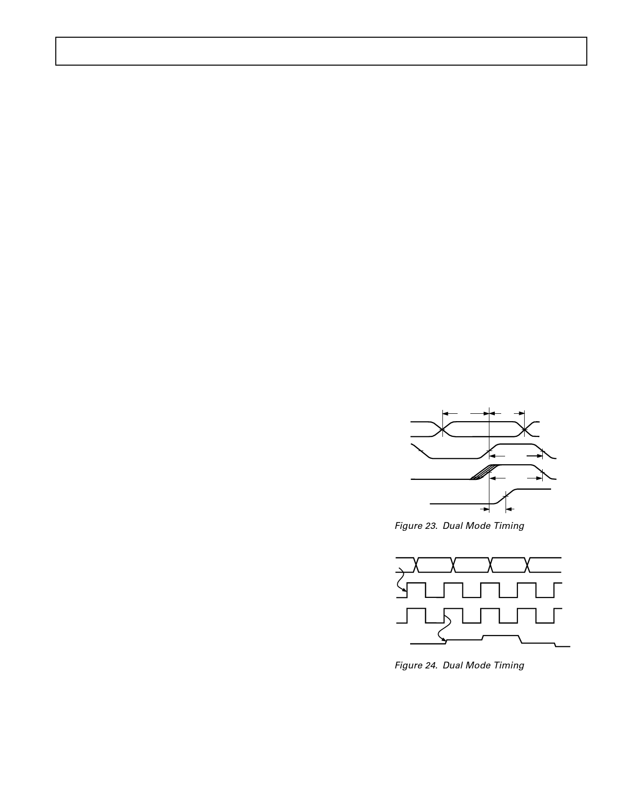
Timing specifications for dual port mode are given in Figures 23
and 24.
DATA IN
tS
tH
WRT1/WRT2
CLK1/CLK2
IOUTA
OR
IOUTB
t LPW
t CPW
t PD
Figure 23. Dual Mode Timing
DATA IN D1
D2
D3
D4
D5
WRT1/WRT2
CLK1/CLK2
IOUTA
OR
IOUTB
xx
D2
D1
D3
D4
Figure 24. Dual Mode Timing
REV. B
–11–
Share Link: 