AS5SS256K36 Просмотр технического описания (PDF) - Micross Components
Номер в каталоге
Компоненты Описание
производитель
AS5SS256K36 Datasheet PDF : 17 Pages
| |||
SSRAM
AS5SS256K36
GENERAL DESCRIPTION (continued)
Asynchronous inputs include the output enable (OE\),
clock (CLK) and snooze enable (ZZ). There is also a burst
mode input (MODE) that selects between interleaved and
linear burst modes. The data-out (Q), enabled by OE\, is also
asynchronous. WRITE cycles can be from one to four bytes
wide as controlled by the write control inputs.
Burst operation can be initiated with either address
status processor (ADSP\) or address status controller (ADSC\)
inputs. Subsequent burst addresses can be internally generated
as controlled by the burst advance input (ADV\).
Address and write control are registered on-chip to
simplify WRITE cycles. This allows self-timed WRITE cycles.
Individual byte enables allow individual bytes to be written.
During WRITE cycles on the x18 device, BWa\ controls DQa’s
and DQPa; BWb\ controls DQb’s and DQPb; BWc\ controls
DQc’s and DQPc; BWd\ controls DQd’s and DQPd. GW\ LOW
causes all bytes to be written. Parity bits are also featured on
this device.
This 8Mb Synchronous Burst SRAM operates from a
+3.3V VDD power supply, and all inputs and outputs are TTL-
compatible. The device is ideally suited for 486, Pentium©,
680x0 and PowerPCTM systems and those systems that benefit
from a wide synchronous data bus.
SA0, SA1, SAs
MODE
ADV\
CLK
ADSC\
ADSP\
BWd\
BWc\
BWb\
BWa\
BWE\
GW\
CE\
CE2
CE2\
OE\
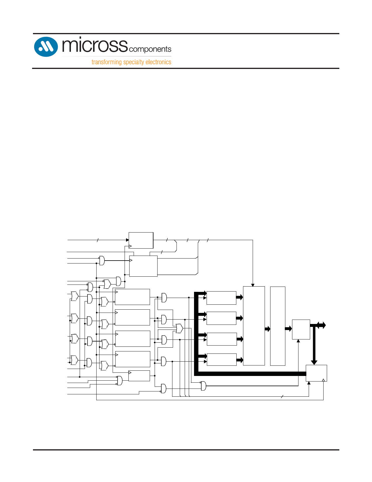
FUNCTIONAL BLOCK DIAGRAM
18
ADDRESS
18
16
18
REGISTER
SA0-SA1
BINARY Q1
COUNTER SA1'
AND LOGIC
CL
Q0
SA0'
BYTE "d"
WRITE REGISTER
BYTE "d"
WRITE DRIVER
BYTE "c"
WRITE REGISTER
BYTE "b"
WRITE REGISTER
BYTE "c"
WRITE DRIVER
BYTE "b"
WRITE DRIVER
256K x 9 x 4
(x36)
MEMORY
ARRAY
SENSE
AMPS
OUTPUT
BUFFERS
DQs
DQPa
DQPb
DQPc
DQPd
BYTE "a"
WRITE REGISTER
ENABLE
REGISTER
BYTE "a"
WRITE DRIVER
INPUT
REGISTERS
4
NOTE: Functional Block Diagrams illustrate simplified device operation. See Truth Table, Pin Descriptions
for detailed information.
and time diagrams
AS5SS256K36
Rev. 4.4 10/13
Micross Components reserves the right to change products or specifications without notice.
2
Share Link: 