MC74LCX373 Просмотр технического описания (PDF) - ON Semiconductor
Номер в каталоге
Компоненты Описание
производитель
MC74LCX373 Datasheet PDF : 9 Pages
| |||
MC74LCX373
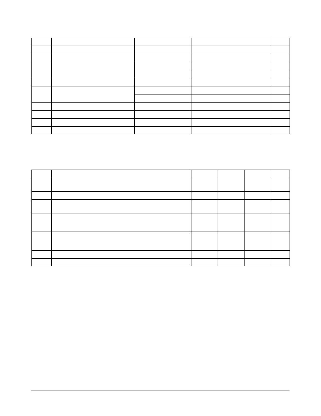
MAXIMUM RATINGS
Symbol
Parameter
Value
Condition
Unit
VCC
DC Supply Voltage
-0.5 to +7.0
V
VI
DC Input Voltage
-0.5 ≤ VI ≤ +7.0
V
VO
DC Output Voltage
-0.5 ≤ VO ≤ +7.0
Output in 3-State
V
-0.5 ≤ VO ≤ VCC + 0.5
Output in HIGH or LOW State (Note 1)
V
IIK
DC Input Diode Current
-50
VI< GND
mA
IOK
DC Output Diode Current
-50
VO < GND
mA
+50
VO > VCC
mA
IO
DC Output Source/Sink Current
±50
mA
ICC
DC Supply Current Per Supply Pin
±100
mA
IGND
DC Ground Current Per Ground Pin
±100
mA
TSTG
Storage Temperature Range
-65 to +150
°C
Stresses exceeding Maximum Ratings may damage the device. Maximum Ratings are stress ratings only. Functional operation above the
Recommended Operating Conditions is not implied. Extended exposure to stresses above the Recommended Operating Conditions may affect
device reliability.
1. IO absolute maximum rating must be observed.
RECOMMENDED OPERATING CONDITIONS
Symbol
Parameter
Min
Typ
Max
Unit
VCC
Supply Voltage
Operating
Data Retention Only
2.0
2.5, 3.3
3.6
V
1.5
2.5, 3.3
3.6
VI
Input Voltage
VO
Output Voltage
0
(HIGH or LOW State)
0
(3-State)
0
5.5
V
VCC
V
5.5
IOH
HIGH Level Output Current
VCC = 3.0 V - 3.6 V
VCC = 2.7 V - 3.0 V
VCC = 2.3 V - 2.7 V
IOL
LOW Level Output Current
VCC = 3.0 V - 3.6 V
VCC = 2.7 V - 3.0 V
VCC = 2.3 V - 2.7 V
TA
Operating Free-Air Temperature
-40
Dt/DV Input Transition Rise or Fall Rate, VIN from 0.8 V to 2.0 V, VCC = 3.0 V
0
- 24
mA
- 12
-8
+ 24
mA
+ 12
+8
+85
°C
10
ns/V
http://onsemi.com
3
Share Link: 