A54SX08A Просмотр технического описания (PDF) - Actel Corporation
Номер в каталоге
Компоненты Описание
производитель
A54SX08A Datasheet PDF : 108 Pages
| |||
SX-A Family FPGAs
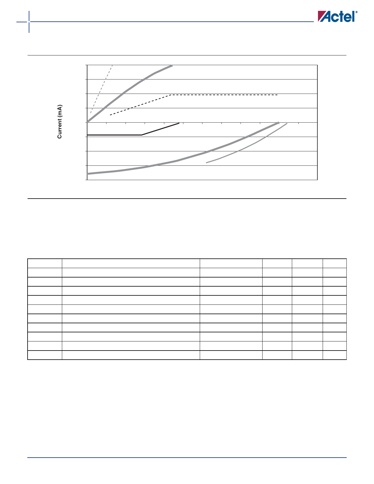
Figure 2-1 shows the 5 V PCI V/I curve and the minimum and maximum PCI drive characteristics of the SX-A family.
200.0
150.0
IOL MAX Spec
100.0
50.0
0.0
0
0.5 1 1.5
–50.0
IOH MIN Spec
–100.0
–150.0
IOH
–200.0
Figure 2-1 • 5 V PCI V/I Curve for SX-A Family
IOH = 11.9 * (VOUT – 5.25) * (VOUT + 2.45)
for VCCI > VOUT > 3.1V
IOL
IOL MIN Spec
2 2.5 3 3.5 4 4.5 5 5.5 6
IOH MAX Spec
Voltage Out (V)
EQ 2-1
IOL = 78.5 * VOUT * (4.4 – VOUT)
for 0V < VOUT < 0.71V
EQ 2-2
Table 2-9 • DC Specifications (3.3 V PCI Operation)
Symbol Parameter
Condition
Min.
Max. Units
VCCA
Supply Voltage for Array
2.25
2.75
V
VCCI
Supply Voltage for I/Os
3.0
3.6
V
VIH
Input High Voltage
0.5VCCI VCCI + 0.5
V
VIL
Input Low Voltage
IIPU
Input Pull-up Voltage1
IIL
Input Leakage Current2
0 < VIN < VCCI
–0.5
0.3VCCI
V
0.7VCCI
–
V
–10
+10
μA
VOH
Output High Voltage
IOUT = –500 µA
0.9VCCI
–
V
VOL
Output Low Voltage
CIN
Input Pin Capacitance3
IOUT = 1,500 µA
0.1VCCI
V
–
10
pF
CCLK
CLK Pin Capacitance
5
12
pF
Notes:
1. This specification should be guaranteed by design. It is the minimum voltage to which pull-up resistors are calculated to pull a
floated network. Designers should ensure that the input buffer is conducting minimum current at this input voltage in applications
sensitive to static power utilization.
2. Input leakage currents include hi-Z output leakage for all bidirectional buffers with tristate outputs.
3. Absolute maximum pin capacitance for a PCI input is 10 pF (except for CLK).
v5.3
2-5
Share Link: 