A54SX08A Просмотр технического описания (PDF) - Actel Corporation
Номер в каталоге
Компоненты Описание
производитель
A54SX08A Datasheet PDF : 108 Pages
| |||

SX-A Family FPGAs
Table 2-8 • AC Specifications (5 V PCI Operation)
Symbol
Parameter
Condition
Min.
Max.
Units
IOH(AC)
Switching Current High
0 < VOUT ≤ 1.4 1
1.4 ≤ VOUT < 2.4 1, 2
3.1 < VOUT < VCCI 1, 3
–44
–
mA
(–44 + (VOUT – 1.4)/0.024)
–
mA
–
EQ 2-1 on
–
page 2-5
IOL(AC)
(Test Point)
Switching Current Low
VOUT = 3.1 3
VOUT ≥ 2.2 1
2.2 > VOUT > 0.55 1
0.71 > VOUT > 0 1, 3
–
95
(VOUT/0.023)
–
–142
mA
–
mA
–
mA
EQ 2-2 on
–
page 2-5
(Test Point)
VOUT = 0.71 3
–
206
mA
ICL
slewR
slewF
Low Clamp Current
Output Rise Slew Rate
Output Fall Slew Rate
–5 < VIN ≤ –1
0.4 V to 2.4 V load 4
2.4 V to 0.4 V load 4
–25 + (VIN + 1)/0.015
1
1
–
mA
5
V/ns
5
V/ns
Notes:
1. Refer to the V/I curves in Figure 2-1 on page 2-5. Switching current characteristics for REQ# and GNT# are permitted to be one half
of that specified here; i.e., half size output drivers may be used on these signals. This specification does not apply to CLK and RST#,
which are system outputs. “Switching Current High” specifications are not relevant to SERR#, INTA#, INTB#, INTC#, and INTD#,
which are open drain outputs.
2. Note that this segment of the minimum current curve is drawn from the AC drive point directly to the DC drive point rather than
toward the voltage rail (as is done in the pull-down curve). This difference is intended to allow for an optional N-channel pull-up.
3. Maximum current requirements must be met as drivers pull beyond the last step voltage. Equations defining these maximums (A
and B) are provided with the respective diagrams in Figure 2-1 on page 2-5. The equation defined maximum should be met by
design. In order to facilitate component testing, a maximum current test point is defined for each side of the output driver.
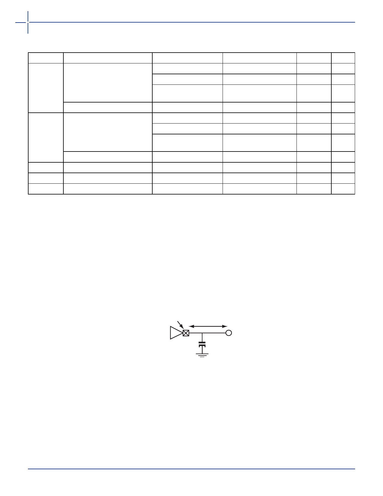
4. This parameter is to be interpreted as the cumulative edge rate across the specified range, rather than the instantaneous rate at any
point within the transition range. The specified load (diagram below) is optional; i.e., the designer may elect to meet this parameter
with an unloaded output per revision 2.0 of the PCI Local Bus Specification. However, adherence to both maximum and minimum
parameters is now required (the maximum is no longer simply a guideline). Since adherence to the maximum slew rate was not
required prior to revision 2.1 of the specification, there may be components in the market for some time that have faster edge
rates; therefore, motherboard designers must bear in mind that rise and fall times faster than this specification could occur and
should ensure that signal integrity modeling accounts for this. Rise slew rate does not apply to open drain outputs.
Pin
Output
Buffer
1/2 in. max.
50 pF
2-4
v5.3