LA4425A Просмотр технического описания (PDF) - ON Semiconductor
Номер в каталоге
Компоненты Описание
производитель
LA4425A Datasheet PDF : 9 Pages
| |||
LA4425A
Instructions and Precautions
• Connect a capacitor of 1000pF across pins and for external disturbance path.
• Be careful of the ground line artwork when laying out the printed circuit pattern. Arrange so that the Sg route and load
current flow-in route do not overlap. Refer to the recommended printed circuit pattern or make slits, etc. at pins
and .
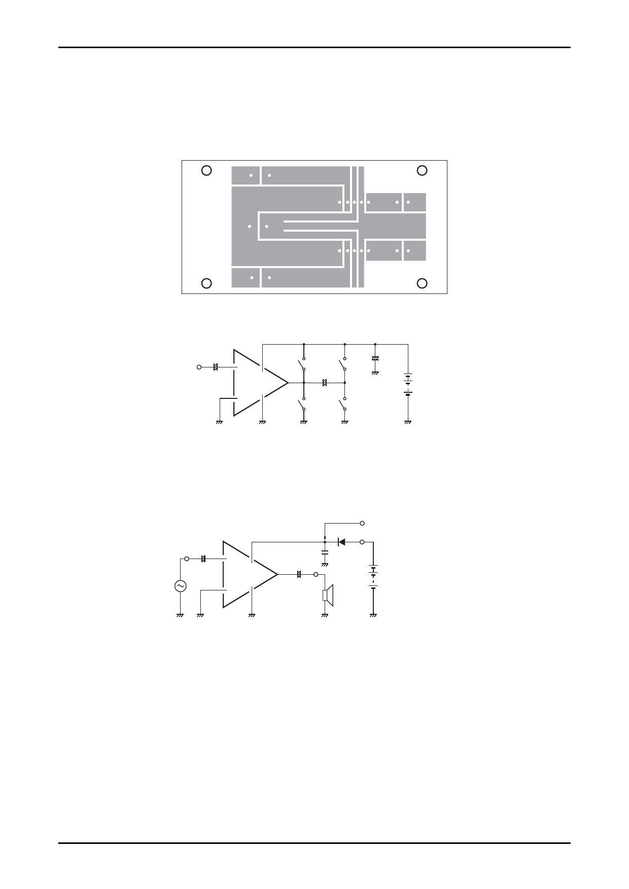
DUAL Printed Circuit Pattern Example
OUT1
VCC
OUT2
GND
1
1
IN1
GND
IN2
• Short Circuit Tests
Cu-foiled side 45.0×75.0mm2
SW1
SW3
+
LA4425A
+
+
13.2V
SW2
SW4
Our company's recommended printed circuit board: Apply VCC=13.2V using a 30×30×1.5mm3 thick aluminum board.
The IC will be protected from the DC/AC shorting of switches 1 to 4 above. However, be careful not to damage the IC
by turning VCC ”ON” when DC short (SW 1 or SW 2) is on.
• Power Supply Positive Surge
JASO tester
Application of giant pulse
2.2μF
+
Rg
620Ω
LA4425A
0.15μF
+
1000μF
RL
13.2V
The over-voltage protector (VCCX ≈ 21.5V) inside the IC is used to cut all bias routes and reverse bias between B-E of
output stage elements, in order to increase the power line’s capability of handling positive surge. This means, of course,
that a VCES (VCBO) type output stage element is used instead of the VCEO (VCER) type.
No.A0195-7/9
Share Link: 