03N06C Просмотр технического описания (PDF) - Harris Semiconductor
Номер в каталоге
Компоненты Описание
производитель
03N06C Datasheet PDF : 13 Pages
| |||
RLD03N06CLE, RLD03N06CLESM, RLP03N06CLE
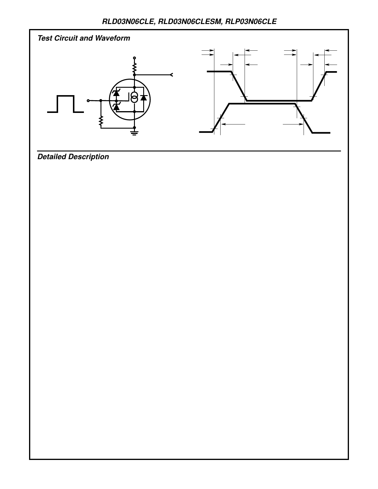
Test Circuit and Waveform
VDD
RL
VDS
VDS
tON
tD(ON)
tR
90%
tOFF
tD(OFF)
tF
90%
VGS
0V
RGS
DUT
10%
VGS
10%
50%
PULSE WIDTH
10%
90%
50%
FIGURE 13. RESISTIVE SWITCHING TEST CIRCUIT
FIGURE 14. RESISTIVE SWITCHING WAVEFORMS
Detailed Description
Temperature Dependence of Current Limiting and
Switching Speed Performance
The RLD03N06CLE, RLD03N06CLESM and RLP03N06CLE
are a monolithic power device which incorporates a Logic Level
power MOSFET transistor with a current sensing scheme and
control circuitry to enable the device to self limit the drain
source current flow. The current sensing scheme supplies cur-
rent to a resistor that is connected across the base to emitter of
a bipolar transistor in the control section. The collector of this
bipolar transistor is connected to the gate of the power MOS-
FET transistor. When the ratiometric current from the current
sensing reaches the value required to forward bias the base
emitter junction of this bipolar transistor, the bipolar “turns on”.
A resistor is incorporated in series with the gate of the power
MOSFET transistor allowing the bipolar transistor to adjust the
drive on the gate of the power MOSFET transistor to a voltage
which then maintains a constant current in the power MOSFET
transistor. Since both the ratiometric current sensing scheme
and the base emitter unction voltage of the bipolar transistor
vary with temperature, the current at which the device limits is a
function of temperature. This dependence is shown in Figure 3.
The resistor in series with the gate of the power MOSFET
transistor also results in much slower switching performance
than in standard power MOSFET transistors. This is an
advantage where fast switching can cause EMI or RFI. The
switching speed is very predictable.
DC Operation
The limit on the drain to source voltage for operation in cur-
rent limiting on a steady state (DC) basis is shown in the
equation below. The dissipation in the device is simply the
applied drain to source voltage multiplied by the limiting cur-
rent. This device, like most power MOSFET devices today, is
limited to 175oC. The maximum voltage allowable can,
therefore, be expressed as shown in Equation 1:
VDS = (--I-1-L--5--M--0---•°---C-(--R--–--θ-T--J-A--C---M--+---B-R--I--Eθ---J-N--A--T--)--)-
(EQ. 1)
The results of this equation are plotted in Figure 15 for vari-
ous heatsinks.
Duty Cycle Operation
In many applications either the drain to source voltage or the
gate drive is not available 100% of the time. The copper
header on which the RLD03N06CLE, RLD03N06CLESM
and RLP03N06CLE is mounted has a very large thermal
storage capability, so for pulse widths of less then 1ms, the
temperature of the header can be considered a constant,
thereby the junction temperature can be calculated simply as
shown in Equation 2:
TC = (VDS • ID • D • RθCA) + TA MBIENT
(EQ. 2)
Generally the heat storage capability of the silicon chip in a
power transistor is ignored for duty cycle calculations. Mak-
ing this assumption, limiting junction temperature to 175oC
and using the TC calculated in Equation 2, the expression for
maximum VDS under duty cycle operation is shown in Equa-
tion 3:
VDS = I--L----1M---5---0-•---o-D--C----•--–--R---T-θ---C-J---C---
(EQ. 3)
These values are plotted as Figures 16 through 21 for vari-
ous heatsink thermal resistances.
Limited Time Operations
Protection for a limited period of time is sufficient for many
applications. As stated above the heat storage in the silicon
chip can usually be ignored for computations of over 10 ms,
thereby the thermal equivalent circuit reduces to a simple
enough circuit to allow easy computation on the limiting con-
ditions. The variation in limiting current with temperature
complicates the calculation of junction temperature, but a
simple straight line approximation of the variation is accurate
enough to allow meaningful computations. The curves
shown as Figures 22 through 25 (RLP03N06CLE) and Fig-
ure 26 through 29 (RLD03N06CLE and RLD03N06CLESM)
give an accurate indication of how long the specified voltage
can be applied to the device in the current limiting mode
without exceeding the maximum specified 175oC junction
temperature. In practice this tells you how long you have to
alleviate the condition causing the current limiting to occur.
5
Share Link: 