USB3318C-CP-TR Просмотр технического описания (PDF) - Microchip Technology
Номер в каталоге
Компоненты Описание
производитель
USB3318C-CP-TR
Microchip Technology

USB3318C-CP-TR Datasheet PDF : 73 Pages
| |||
Hi-Speed USB Transceiver with 1.8V-3.3V ULPI Interface - 13MHz Reference Clock
Datasheet
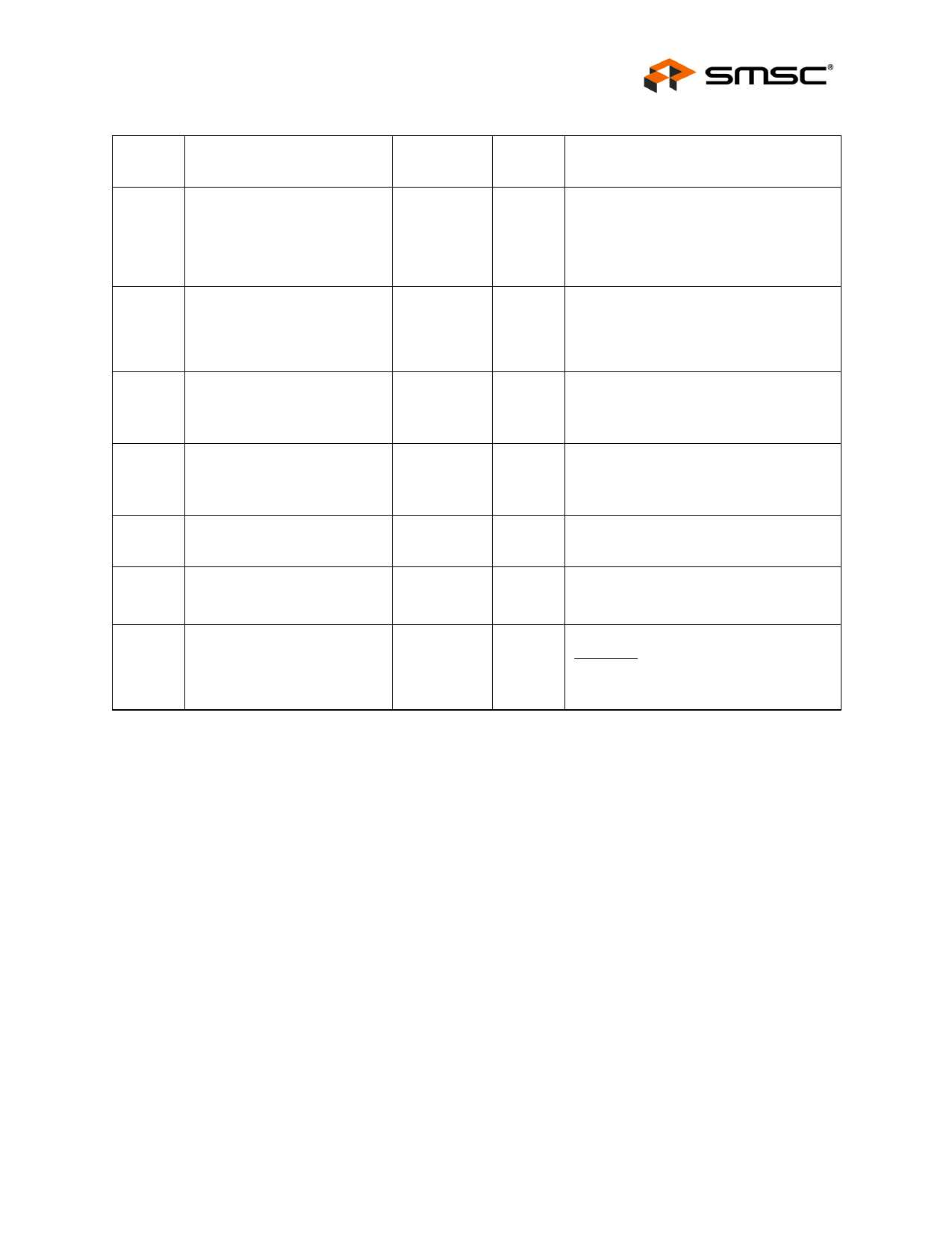
Table 2.1 USB3318 Pin Description (continued)
PIN
DIRECTION/ ACTIVE
NAME
TYPE
LEVEL
DESCRIPTION
19
DIR
Output,
N/A Controls the direction of the data bus.
CMOS
When the PHY has data to transfer to the
Link, it drives DIR high to take ownership
of the bus. When the PHY has no data to
transfer it drives DIR low and monitors
the bus for commands from the Link.
20
STP
Input,
High The Link asserts STP for one clock cycle
CMOS
to stop the data stream currently on the
bus. If the Link is sending data to the
PHY, STP indicates the last byte of data
was on the bus in the previous cycle.
21
VDD1.8
Power
N/A External 1.8V Supply input pin. This pad
needs to be bypassed with a 0.1uF
capacitor to ground, placed as close as
possible to the USB3318.
22
RESETB
Input,
N/A When low, the part is suspended with all
CMOS,
of the I/O tri-stated. When high the
USB3318 will operate as a normal ULPI
device.
23
REFCLK
Input,
N/A 13MHz Reference Clock input.
CMOS
24
FLAG
RBIAS
GND
Analog,
CMOS
Ground
N/A Rbias pin. This pin requires an 8.06kΩ
(±1%) resistor to ground, placed as close
as possible to the USB3318.
N/A Ground.
QFN only: The flag should be connected
to the ground plane with a via array
under the exposed flag. This is the main
ground for the IC.
SMSC USB3318 REV C
11
DATASHEET
Revision 2.1 (06-02-10)
Share Link: