IDT70V05L(1996) Просмотр технического описания (PDF) - Integrated Device Technology
Номер в каталоге
Компоненты Описание
производитель
IDT70V05L Datasheet PDF : 17 Pages
| |||
IDT70V05S/L
HIGH-SPEED 3.3V 8K x 8 DUAL-PORT STATIC RAM
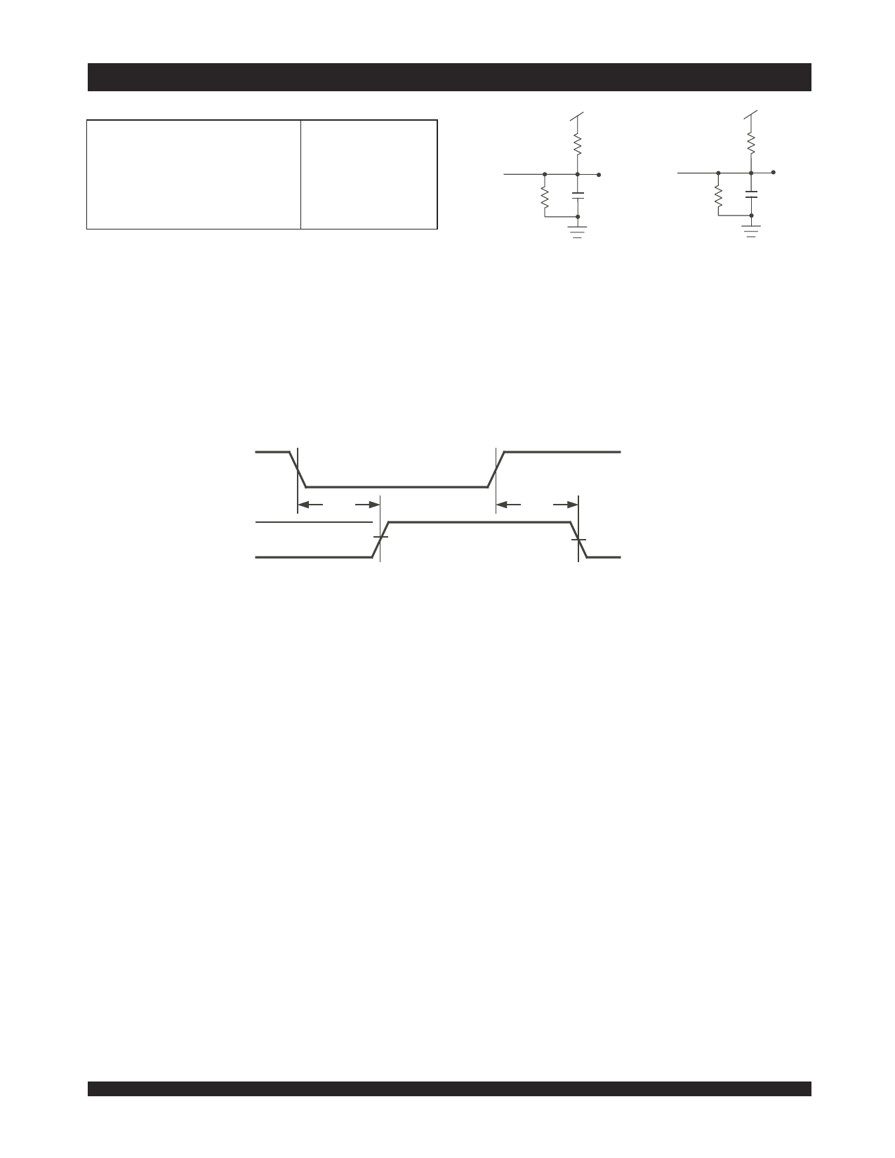
WAVEFORM OF READ CYCLES(5)
ADDR
CE
OE
tRC
tAA (4)
tACE (4)
tAOE (4)
COMMERCIAL TEMPERATURE RANGE
R/W
DATAOUT
BUSYOUT
tLZ (1)
VALID DATA (4)
tBDD (3, 4)
tOH
tHZ (2)
2941 drw 08
NOTES:
1. Timing depends on which signal is asserted last, OE or CE.
2. Timing depends on which signal is de-asserted first, CE or OE.
3. tBDD delay is required only in cases where the opposite port is completing a write operation to the same address location. For simultaneous read operations
BUSY has no relation to valid output data.
4. Start of valid data depends on which timing becomes effective last tAOE, tACE, tAA or tBDD.
5. SEM = VIH.
AC ELECTRICAL CHARACTERISTICS OVER THE
OPERATING TEMPERATURE AND SUPPLY VOLTAGE(5)
IDT70V05X25
IDT70V05X35
IDT70V05X55
Symbol
Parameter
Min.
Max.
Min.
Max.
Min.
Max. Unit
WRITE CYCLE
tWC
Write Cycle Time
tEW
Chip Enable to End-of-Write(3)
25
—
35
—
55
—
ns
20
—
30
—
45
—
ns
tAW
Address Valid to End-of-Write
tAS
Address Set-up Time(3)
20
—
30
—
45
—
ns
0
—
0
—
0
—
ns
tWP
Write Pulse Width
20
—
25
—
40
—
ns
tWR
Write Recovery Time
0
—
0
—
0
—
ns
tDW
tHZ
tDH
tWZ
tOW
tSWRD
tSPS
Data Valid to End-of-Write
Output High-Z Time(1, 2)
Data Hold Time(4)
Write Enable to Output in High-Z(1, 2)
Output Active from End-of-Write(1, 2, 4)
SEM Flag Write to Read Time
SEM Flag Contention Window
15
—
20
—
30
—
ns
—
15
—
20
—
25
ns
0
—
0
—
0
—
ns
—
15
—
20
—
25
ns
0
—
0
—
0
—
ns
5
—
5
—
5
—
ns
5
—
5
—
5
—
ns
NOTES:
2941 tbl 12
1. Transition is measured ±200mV from Low or High-impedance voltage with Output Test Load (Figure 2).
2. This parameter is guaranteed by device characterization but not production tested.
3. To access RAM, CE = VIL, SEM = VIH. To access semaphore, CE = VIH and SEM = VIL. Either condition must be valid for the entire tEW time.
4. The specification for tDH must be met by the device supplying write data to the RAM under all operating conditions. Although tDH and tOW values will vary
over voltage and temperature, the actual tDH will always be smaller than the actual tOW.
5. "X" in part numbers indicates power rating (S or L).
6.35
7
Share Link: 