ADDC02808PBTV(Rev0) Просмотр технического описания (PDF) - Analog Devices
Номер в каталоге
Компоненты Описание
производитель
ADDC02808PBTV Datasheet PDF : 20 Pages
| |||
ADDC02808PB
8.1
RESR = 10 mΩ. The di/dt is 12 A/µs. As can be seen, the peak
deviations for these curves are close to each other and
8
comparable to the negative deviation shown in Figure 6 for
7.9
a similarly sized positive step change in load current.
7.8
7.7
100
90
100mV
VO
7.6
7.5
10
7.4
0%
OBSOLETE –200 –100 0 100 200 300 400 500 600 700 800
TIME – µs
Figure 25. Predicted Response for 24 A Step Load Change,
di/dt = 12 A/µs, with Factory Set Internal Compensation
Optimized for CLOAD = 4,000 µF and RESR = 2.5 mΩ
RESPONSE AT END OF PULSE
The previous section describes how the ADDC02808PB
converter responds to the positive step change in load current
that occurs at the beginning of a power pulse. This section will
discuss the converter’s response at the end of the power pulse
when the load current is abruptly returned to a small value.
Figures 26-29 show the converter’s measured output voltage as
the load current is stepped from 25 A down to 4 A, 2 A, 1 A, and
0.1 A, respectively. The load capacitance is 1,000 µF with
100µs
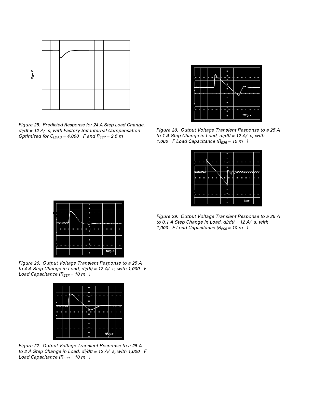
Figure 28. Output Voltage Transient Response to a 25 A
to 1 A Step Change in Load, di/dt/ = 12 A/µs, with
1,000 µF Load Capacitance (RESR = 10 mΩ)
100
90
100mV
VO
10
0%
1ms
100
100mV 90
VO
10
0%
100µs
Figure 26. Output Voltage Transient Response to a 25 A
to 4 A Step Change in Load, di/dt/ = 12 A/µs, with 1,000 µF
Load Capacitance (RESR = 10 mΩ)
100
100mV 90
VO
10
0%
100µs
Figure 29. Output Voltage Transient Response to a 25 A
to 0.1 A Step Change in Load, di/dt/ = 12 A/µs, with
1,000 µF Load Capacitance (RESR = 10 mΩ)
What is different about these curves is the settling time. Once
the converter’s output voltage rises above nominal, the
converter cannot help to discharge the load capacitor. It can
only reduce its output current to zero; it cannot draw a negative
current. As such, the time it takes to bring the output voltage
back down to its nominal value depends on the load current
during the low load portion of the cycle. The rate at which the
output voltage falls to its nominal value is the load current
divided by the load capacitance (including the 150 µF
capacitance that is inside the converter). The smaller the load
current, the longer it takes to get the output voltage back to its
nominal value.
During the time that the output voltage is too high, the
integrator in the converter’s feedback circuitry is continuing to
ramp out of range. As the output voltage then falls below its
nominal value, it must have an undershoot error to bring the
integrator back into range. As can be seen from these figures,
the lower the load current, the longer the output voltage
remains too high, and the longer and the greater the output
voltage undershoot is.
Figure 27. Output Voltage Transient Response to a 25 A
to 2 A Step Change in Load, di/dt/ = 12 A/µs, with 1,000 µF
Load Capacitance (RESR = 10 mΩ)
Even when the load current steps down to 0.1 A, the maximum
deviation of the output voltage is only about 400 mV, or 5%.
However, it is important to realize that if the next power pulse
occurs before this transient is over, then the output voltage will
–10–
REV. 0
Share Link: 