ADDC02808PBTV(Rev0) Просмотр технического описания (PDF) - Analog Devices
Номер в каталоге
Компоненты Описание
производитель
ADDC02808PBTV Datasheet PDF : 20 Pages
| |||
ADDC02808PB
250
200
100W ave
150
MAXIMUM PEAK
POWER LIMIT
10W ave
50W ave
100
MAXIMUM CONTINUOUS
POWER LIMIT
50
8.1
8
7.9
7.8
12A STEP CHANGE
7.7
24A STEP CHANGE
7.6
7.5
7.4
0
–200 –100 0 100 200 300 400 500 600 700 800
OBSOLETE 0
25
50
75
100
125
150
PULSE WIDTH – ms
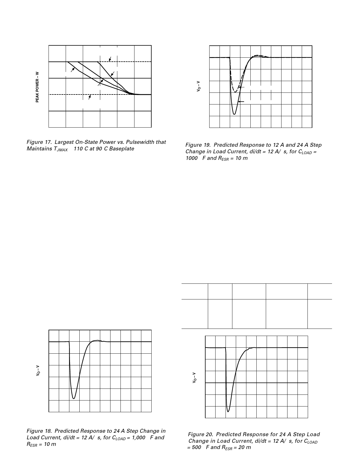
Figure 17. Largest On-State Power vs. Pulse Width that
Maintains TJMAX ≤ 110°C at 90°C Baseplate
TRANSIENT RESPONSE
The standard ADDC02808PB is designed to deliver large
changes, or pulses, in load current with minimum output
voltage deviation and an ultrafast return to the nominal output
voltage. The compensation of the feedback loop is optimized,
and output stability is insured, for a broad range of external load
capacitance extending from 500 µF (RESR = 20 mΩ) to 4,000 µF
(RESR = 2.5 mΩ). The variables that impact pulse performance
(the maximum output voltage deviation and the settling time)
are:
1. Size of step change in the output current.
2. Amount of external load capacitance.
TIME – µs
Figure 19. Predicted Response to 12 A and 24 A Step
Change in Load Current, di/dt = 12 A/µs, for CLOAD =
1000 µF and RESR = 10 mΩ
Step Change
If the step change is less than 24 A, the pulse response will im-
prove. For instance, with a 12 A step change, Figure 19 shows
a comparison of the response for a 24 A step change and a 12 A
step change in load.
Load Capacitance
Varying the external load capacitance and associated RESR be-
tween the range of CLOAD = 500 µF (RESR = 20 mΩ) and CLOAD
= 4,000 µF (RESR = 2.5 mΩ) results in the predicted waveforms
shown in Figures 20, 21, and 22. As can be seen, the larger the
capacitor, the smaller the deviation, but the longer the settling
time. Table I lists the maximum output voltage deviations and
3. Internal compensation of the feedback loop (factory set).
4. Connection from converter output to load.
Extensive modeling of the converter with ADI proprietary
software permits analysis and prediction of the impact each of
these parameters has on the pulse response. The analyses in this
settling times for the four combinations of CLOAD and RESR men-
tioned above. Note that these are based on the standard com-
pensation for the feedback loop.
Table I. Output Response to a 24 A (1 A–25 A) Step in Load
Current (Standard Compensation)
data sheet are based on the load capacitance being comprised of
100 µF, 100 mΩ tantalum load capacitors such as the CSR21
style. Figure 18 is the prediction of the standard converter’s
CLOAD
RESR
Typical
Settling Time See
Deviation (Within 1%) Figure
response to a 24 A step change in load current (from 1 A to
500 µF 20 mΩ –7%
150 µs
20
25 A) with a load capacitance of 1,000 µF (RESR = 10 mΩ).
1,000 µF 10 mΩ –6%
175 µs
18
This is very close to the measured pulse response under the
2,000 µF 5 mΩ
–5%
200 µs
21
same conditions shown in Figure 6.
4,000 µF 2.5 mΩ –4%
250 µs
22
8.1
8.1
8
8
7.9
7.9
7.8
7.8
7.7
7.7
7.6
7.6
7.5
7.4
–200 –100 0 100 200 300 400 500 600 700 800
TIME – µs
Figure 18. Predicted Response to 24 A Step Change in
Load Current, di/dt = 12 A/µs, for CLOAD = 1,000 µF and
RESR = 10 mΩ
7.5
7.4
–200 –100 0 100 200 300 400 500 600 700 800
TIME – µs
Figure 20. Predicted Response for 24 A Step Load
Change in Load Current, di/dt = 12 A/µs, for CLOAD
= 500 µF and RESR = 20 mΩ
–8–
REV. 0
Share Link: 