MC44602 Просмотр технического описания (PDF) - ON Semiconductor
Номер в каталоге
Компоненты Описание
производитель
MC44602 Datasheet PDF : 18 Pages
| |||
MC44602
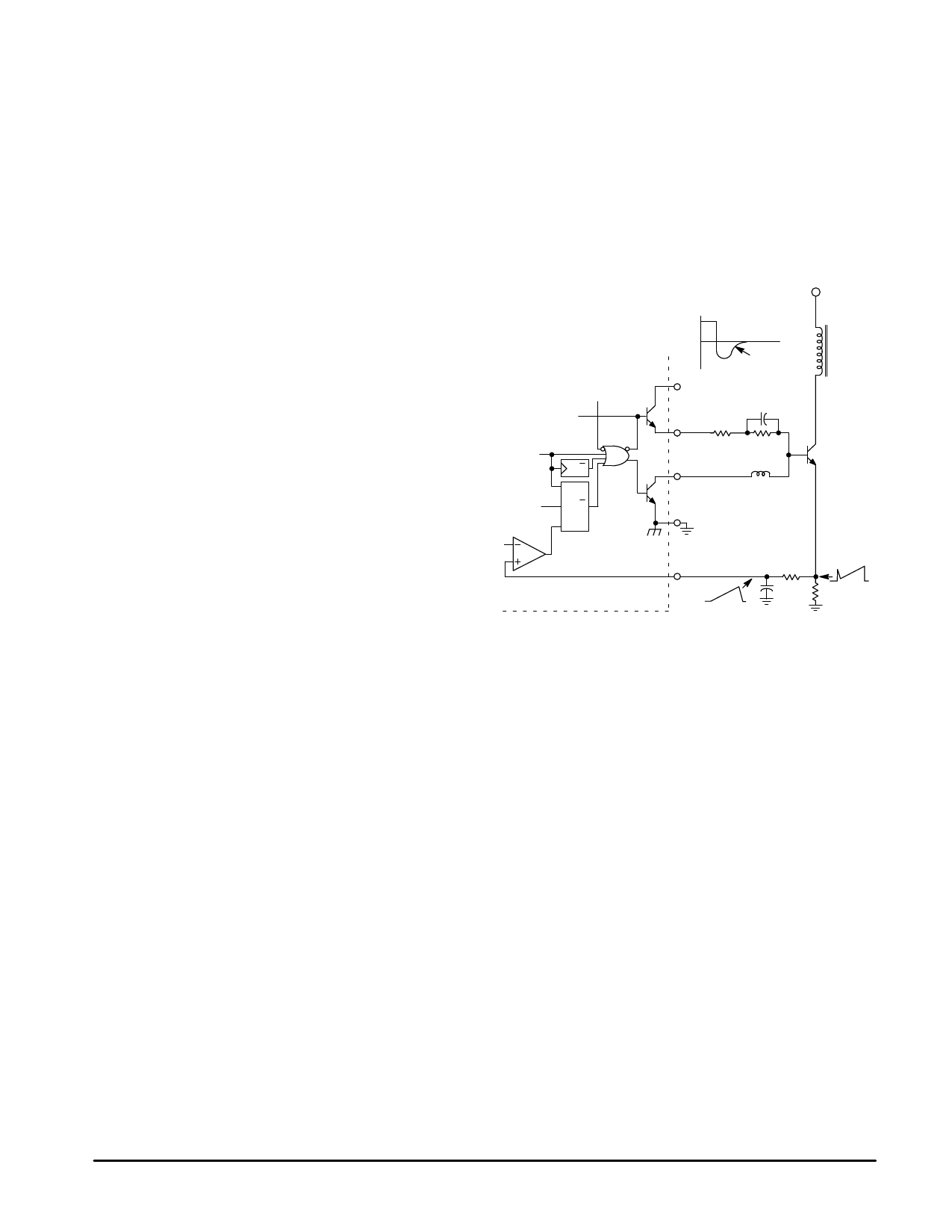
A narrow spike on the leading edge of the current
waveform can usually be observed and may cause the power
supply to exhibit an instability when the output is lightly
loaded. This spike is due to the power transformer
interwinding capacitance and the output rectifier recovery
time. The addition of an RC filter on the Current Sense Input
with a time constant that approximates the spike duration will
usually eliminate the instability; refer to Figure 30.
Undervoltage Lockout
Two undervoltage lockout comparators have been
incorporated to guarantee that the IC is fully functional before
the output stage is enabled. The positive power supply
terminal (VCC) and the reference output (Vref) are each
monitored by separate comparators. Each has built–in
hysteresis to prevent erratic output behavior as their
respective thresholds are crossed. The VCC comparator
upper and lower thresholds are 14.1 V/10.2 V. The Vref
comparator upper and lower thresholds are 3.6 V/3.3 V. The
large hysteresis and low startup current of the MC44602
make it ideally suited for off–line converter applications
(Figures 33, 34) where efficient bootstrap startup techniques
are required.
A 20 V zener is connected as a shunt regulator from VCC to
ground. Its purpose is to protect the IC from excessive
voltage that can occur during system startup. The upper limit
for the minimum operating voltage of the MC44602 is 11V.
Outputs
The MC44602 contains a high current split totem pole
output that was specifically designed for direct drive of
Bipolar Power Transistors. By splitting the totem pole into
separate source and sink outputs, the power supply designer
has the ability to independently adjust the turn–on and
turn–off base drive to the external power transistor for optimal
switching. The Source and Sink outputs are capable of up to
1.0 A and 1.5 A respectively and feature 50 ns switching
times with a 1.0 nF load. Additional internal circuitry has been
added to keep the Source Output “Off” and the Sink Output
“On” whenever an undervoltage lockout is active. This
feature eliminates the need for an external pull–down resistor
and guarantees that the power transistor will be held in the
“Off” state.
Separate output stage power and ground pins are
provided to give the designer added flexibility in tailoring the
base drive circuitry for a specific application. The Source
Output high–state is controlled by applying a positive voltage
to VC (Pin 14) and is independent of VCC. A zener clamp is
typically connected to this input when driving power
MOSFETs in systems where VCC is greater than 20V. The
Sink Output low–state is controlled by applying a negative
voltage to the Sink Ground (Pins 4, 5, 12, 13). The Sink
Ground can be biased as much as 5.0 V negative with
respect to Ground (Pin 7). Proper implementation of the VC
and Sink Ground pins will significantly reduce the level of
switching transient noise imposed on the control circuitry.
This becomes particularly useful when reducing the Ipk(max)
clamp level.
Reference
The 5.0 V bandgap reference has a tolerance of ±6.0%
over a junction temperature range of –25°C to 85°C. Its
primary purpose is to supply charging current to the oscillator
timing capacitor. The reference has short circuit protection
and is capable of providing in excess of 20 mA for powering
additional control system circuitry.
Figure 30. Bipolar Transistor Drive
and Current Spike Suppression
Vin
TQ
S
RQ
R
PWM
Latch
Current Sense
Comparator
IB
+
0
–
Base Charge
VC
Removal
14
CB
Source
11
RB1 RB2
Q1
Sink
10
LB
Sink Gnd
Substrate 4, 5, 12, 13
Current Sense
R
6
C RS
Thermal Protection and Package
Internal Thermal Shutdown circuitry is provided to protect
the integrated circuit in the event that the maximum junction
temperature is exceeded. When activated, typically at 160°C,
the PWM Latch is held in the “reset” state, forcing the Source
Output “Off” and the Sink Output “On”. This feature is
provided to prevent catastrophic failures from accidental
device overheating. It is not intended to be used as a
substitute for proper heatsinking.
The MC44602 is contained in a heatsinkable 16–lead
plastic dual–in–line package in which the die is mounted on a
special heat tab copper alloy lead frame. This tab consists of
the four center Sink Ground pins that are specifically
designed to improve the thermal conduction from the die to
the circuit board. Figure 14 shows a simple and effective
method of utilizing the printed circuit medium as a heat
dissipater by soldering these pins to an adequate area of
copper foil. This permits the use of standard layout and
mounting practices while having the ability to halve the
junction to air thermal resistance. This example is for a
symmetrical layout on a single–sided board with two ounce
per square foot of copper.
MOTOROLA ANALOG IC DEVICE DATA
11
Share Link: 