MC44602 Просмотр технического описания (PDF) - ON Semiconductor
Номер в каталоге
Компоненты Описание
производитель
MC44602 Datasheet PDF : 18 Pages
| |||
MC44602
Design Considerations
Do not attempt to construct the converter on
wire–wrap or plug–in prototype boards. High frequency
circuit layout techniques are imperative to prevent
pulse–width jitter. This is usually caused by excessive noise
pick–up imposed on the Current Sense or Voltage Feedback
inputs. Noise immunity can be improved by lowering circuit
impedances at these points. The printed circuit layout should
contain a ground plane with low–current signal, and high
current switch and output grounds returning on separate
paths back to the input filter capacitor. Ceramic bypass
capacitors (0.1 µF) connected directly to VCC, VC, and
Vref may be required depending upon circuit layout. This
provides a low impedance path for filtering the high frequency
noise. All high current loops should be kept as short as
possible using heavy copper runs to minimize radiated EMI.
The Error Amp compensation circuitry and the converter
output voltage divider should be located close to the IC and
as far as possible from the power switch and other noise
generating components.
PROTECTION MODES
The MC44602 operates as a conventional fixed frequency
current mode controller when the power supply output load is
less than the design limit. For enhanced system reliability, this
device has the unique ability of changing operating modes if
the power supply output is overloaded or shorted.
Overload Protection
Power supply overload protection is provided by the
Foldback Amplifier. As the output load gradually increases,
the Error Amplifier senses that the voltage at Pin 3 is less than
the 2.5 V threshold. This causes the voltage at Pin 1 to rise,
increasing the Current Sense Comparator threshold in order
to maintain output regulation. As the load further increases,
the inverting input of the Current Sense Comparator reaches
the internal 1.0 V clamp level, limiting the switch current to the
calculated Ipk(max). At this point any further increase in load
will cause the power supply output to fall out of regulation. As
the voltage at Pin 3 falls below 2.5 V, current will flow out of
the Foldback Amplifier input, and the internal clamp level will
be proportionally reduced (Figures 9, 10). The increase in
current flowing out of the Foldback Amplifier input in
conjunction with the reduced clamp level, causes the power
supply output voltage to fall at a faster rate than the voltage at
Pin 3. This results in the output foldback characteristic shown
in Figure 31. The shape of the current limit “knee” can be
modified by the value of resistor R1 in the feedback divider.
Lower values of R1 will reduce the Ipk(max) clamp level at a
faster rate.
Improper operation of the Foldback Amp can be
encountered when the Error Amp compensation capacitor Cf
exceeds 2.0 nF. The problem appears at Startup when the
output voltage of the power supply is below nominal, causing
the Error Amp output to rise quickly. The rapid change in
output voltage will be coupled through Cf to the Inverting Input
(Pin 3), keeping it at its 2.5 V threshold as the 1.0 mA Error
Amp current source charges Cf. This has the effect of
disabling the Foldback Amp by preventing Pin 3 and the
clamp level at the inverting input of the Current Sense
Comparator, from rising in proportion to the power supply
output voltage. By adding resistor RFB in series with Cf, the
voltage at Pin 3 can be held to 1.0 V, corresponding to a
Current Sense clamp level of 0.08 V (Figure 10), while
allowing the Error Amp output to reach its high state VOH of
7.0 V. The required resistor to keep Pin 3 below 1.0 V during
initial Startup is:
RFB Rf
RFB + Rf
≥6
R1 R2
R1 + R2
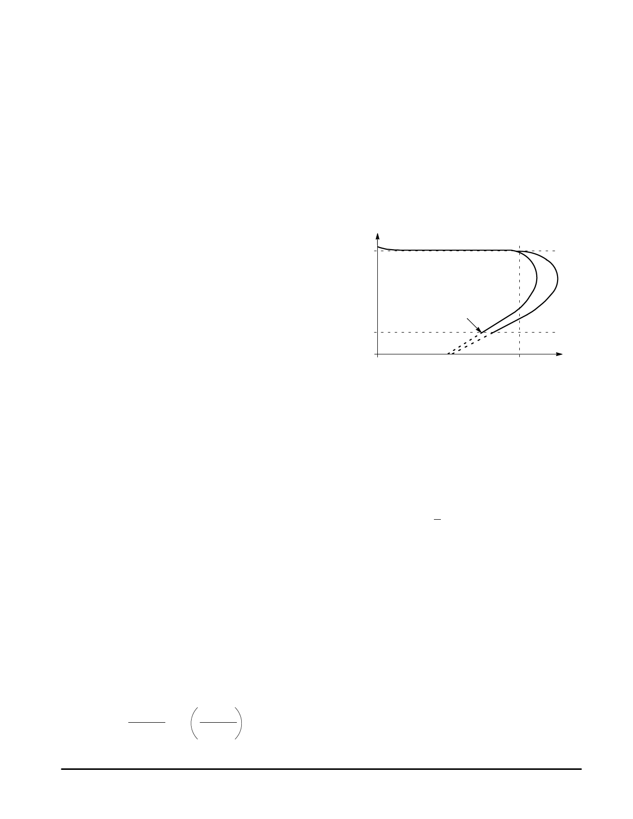
Figure 31. Output Foldback Characteristic
Vout
VO Nominal
lpk(max)
VCC UVLO
Threshold
New Startup
Low Value R1
Sequence Initiated
High Value R1
Nominal Load
Range
Overload Iout
Short Circuit Protection
Short circuit protection for the power supply is provided by
the Valid Load Comparator, Fault Latch, and Demag
Comparator. Figure 32 shows the logic truth table of the
functional blocks. When operating the power supply with
nominal output loading, the Fault Latch is “Set” by the NOR
gate driver during the Power Transistor “On” time and “Reset”
by the Fault Comparator during the “Off” time. When a severe
overload or short circuit occurs on any output, the voltage
during the “Off” time (flyback voltage) at the Load Detect
Input, is unable to reach the 2.5 V threshold of the Valid Load
Comparator. This causes the Fault Latch to remain in the
“Set” state with output Q “Low”. During the “Off” time the
Demag Comparator output will also be “Low”. This causes
the NOR gate to internally hold the Sync Input “High”,
inhibiting the next fixed frequency Oscillator cycle and
switching of the Power Transistor. As the load dissipates the
stored transformer energy, the voltage at the Load Detect
Input will fall. When this voltage reaches 85 mV, the Demag
Comparator output goes “High”, allowing the Sync Input to go
“Low”, and the Power Transistor to turn “On”.
Note that as long as there is an output short, the switching
frequency will shift to a much lower frequency than that set by
RT/CT. The frequency shift has the effect of lowering the duty
cycle, resulting in a significant reduction in Power Transistor
and Output Rectifier heating when compared to conventional
current mode controllers. The extended “On” time is the result
of CT charging from 0 V to 2.8 V instead of 1.2 V to 2.8 V. The
extended “Off” time is the result of the output short time
constant. The time constant consists of the output filter
capacitance, and the equivalent series resistance (ESR) of
the capacitor plus the associated wire resistance.
12
MOTOROLA ANALOG IC DEVICE DATA
Share Link: 