AD6459 Просмотр технического описания (PDF) - Analog Devices
Номер в каталоге
Компоненты Описание
производитель
AD6459 Datasheet PDF : 12 Pages
| |||
ABSOLUTE MAXIMUM RATINGS1
Supply Voltage VPS1, VPS2 to COM1, COM2 . . . . . +5.5 V
Internal Power Dissipation2 . . . . . . . . . . . . . . . . . . . 600 mW
Operating Temperature Range . . . . . . . . . . . –40°C to +85°C
Storage Temperature Range . . . . . . . . . . . . –65°C to +150°C
Lead Temperature, Soldering (60 sec) . . . . . . . . . . . . +300°C
NOTES
1Stresses above those listed under “Absolute Maximum Ratings” may cause
permanent damage to the device. This is a stress rating only, and functional
operation of the device at these or any other conditions above those indicated in the
operational section of this specification is not implied. Exposure to absolute
maximum rating conditions for extended rating conditions for extended periods
may affect device reliability.
2Thermal Characteristics: 20-lead SSOP package: θJA = 126°C/W.
ORDERING GUIDE
Model
AD6459ARS
Temperature
Range
–25°C to +85°C
for 2.7 V to 5.5 V
–40°C to +85°C
for 3.3 V to 5.5 V
Package
Package
Description Option
20-Pin Plastic RS-20
SSOP
AD6459
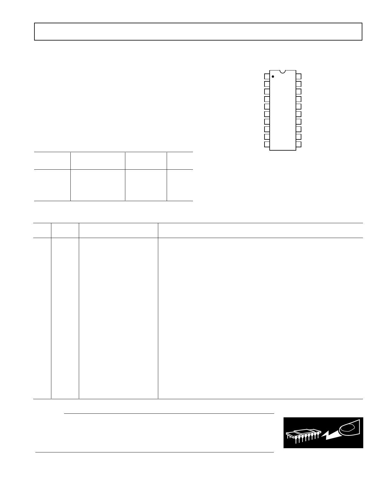
PIN CONNECTION
20-Pin SSOP (RS-20)
FREF 1
20 VPS1
COM1 2
19 FLTR
PRUP 3
18 VPS2
LOIP 4
17 IRXP
RFLO 5 AD6459 16 IRXN
RFHI
6
TOP VIEW
(Not to Scale)
15
QRXP
COM2 7
14 QRXN
GREF 8
13 GAIN
MXOP 9
12 IFIM
MXOM 10
11 IFIP
PIN DESCRIPTIONS
Pin
Pin Label
Description
Function
1
FREF Frequency Reference Input Demodulation LO Input. May either be 3 V CMOS input or >100 mV p-p.
AC-coupled for lowest stand by current.
2
COM1 Common 1
Ground.
3
PRUP Power Up Input
CMOS Compatible Power-Up Control; <1.5 V = OFF, >1.5 V = ON.
4
LOIP Local Oscillator Input
AC-Coupled LO Input. 50 mV p-p drive needed, 500 mV p-p max.
5
RFLO RF “Low” Input
Mixer Differential Input. AC-coupled.
6
RFHI RF “High” Input
Mixer Differential Input. AC-coupled.
7
COM2 Common 2
Ground.
8
GREF Gain Reference Input
High Impedance Input. Sets gain scaling, typically 1.2 V.
9
MXOP Mixer Output “Plus”
Differential Output of the Mixer. See Figure 22.
10 MXOM Mixer Output “Minus”
Differential Output of the Mixer. See Figure 22.
11 IFIP
IF Input “Plus”
Differential Input of Variable Gain Amplifier. AC-coupled.
12 IFIM IF Input “Minus”
Differential Input of Variable Gain Amplifier. AC-coupled.
13 GAIN Gain Control Input
0.2 V–2.4 V Using 3 V Supply. Max gain at 0.2 V.
14 QRXN Q Output “Negative”
Differential Q Output. Output resistance 4.7 kΩ.
15 QRXP Q Output “Positive”
Differential Q Output. Output resistance 4.7 kΩ.
16 IRXN I Output “Negative”
Differential I Output. Output resistance 4.7 kΩ.
17 IRXP I Output “Positive”
Differential I Output. Output resistance 4.7 kΩ.
18 VPS2 VPOS Supply 2
Supply Voltage.
19 FLTR PLL Loop Filter
Series RC Loop Filter. Connected to VPS2.
20 VPS1 VPOS Supply 1
Supply Voltage.
CAUTION
ESD (electrostatic discharge) sensitive device. Electrostatic charges as high as 4000 V readily
accumulate on the human body and test equipment and can discharge without detection.
Although the AD6459 features proprietary ESD protection circuitry, permanent damage may
occur on devices subjected to high energy electrostatic discharges. Therefore, proper ESD
precautions are recommended to avoid performance degradation or loss of functionality.
WARNING!
ESD SENSITIVE DEVICE
REV. 0
–3–
Share Link: 