SST89E554 Просмотр технического описания (PDF) - Silicon Storage Technology
Номер в каталоге
Компоненты Описание
производитель
SST89E554 Datasheet PDF : 58 Pages
| |||
FlashFlex51 MCU
SST89E564 / SST89V564 / SST89E554 / SST89V554
Preliminary Specifications
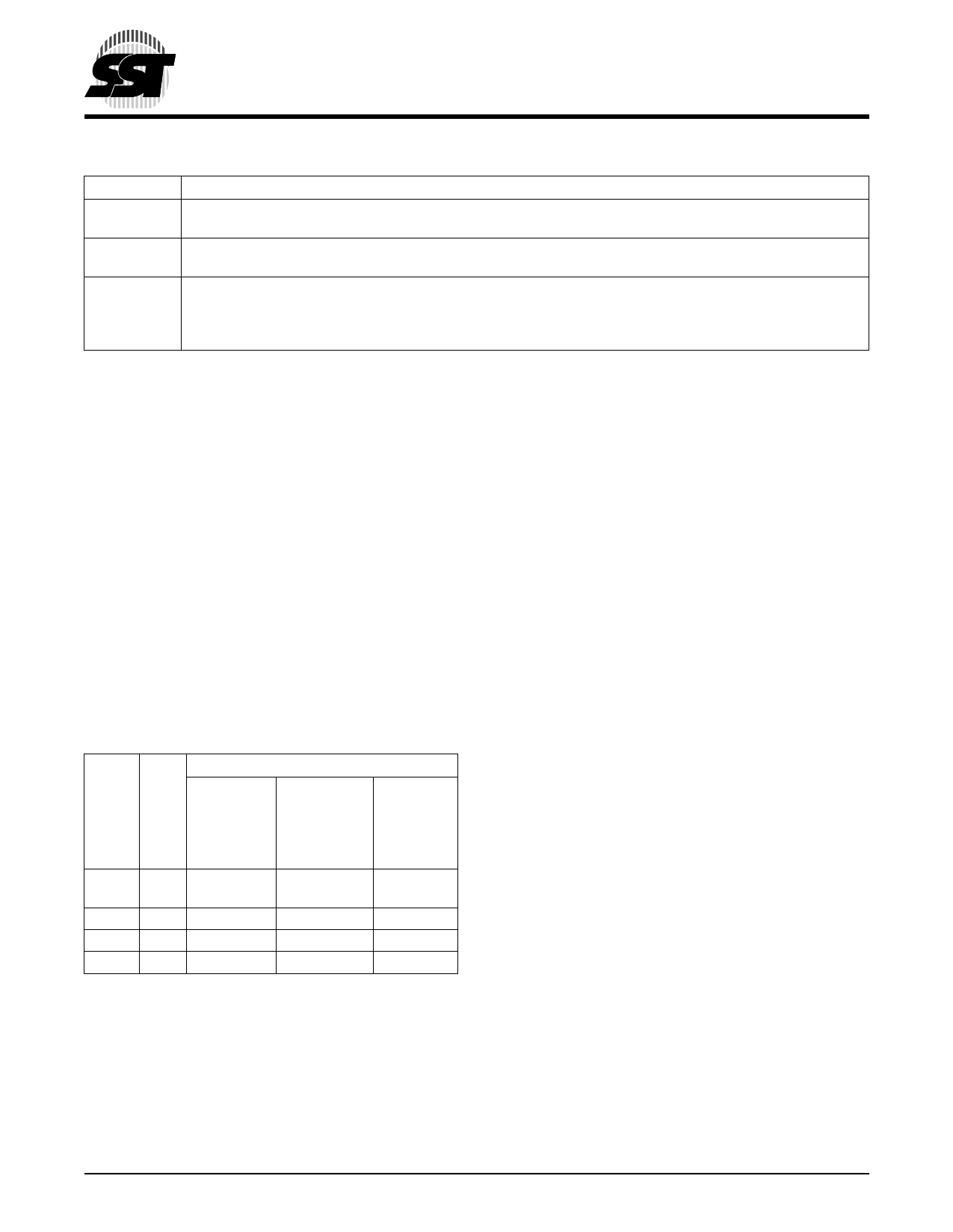
TABLE 3-2: SFCF VALUES FOR PROGRAM MEMORY BLOCK SWITCHING FOR SST89E554/SST89V554
SFCF[1:0]
10, 11
01
00
Program Memory Block Switching
Block 1 is not visible to the PC;
Block 1 is reachable only via In-Application Programming from E000H - FFFFH.
Both Block 0 and Block 1 are visible to the PC.
Block 0 is occupied from 0000H - 7FFFH. Block 1 is occupied from E000H - FFFFH.
Block 1 is overlaid onto the low 8K of the program address space; occupying address locations 0000H - 1FFFH.
When the PC falls within 0000H - 1FFFH, the instruction will be fetched from Block 1 instead of Block 0.
Outside of 0000H - 1FFFH, Block 0 is used. Locations 0000H - 1FFFH of Block 0 are reachable through
In-Application Programming.
T3-2.2 384
3.2.1 Reset Configuration of Program Memory
Block Switching
Program memory block switching is initialized after reset
according to the state of the Start-up Configuration bit SC0.
The SC0 bit is programmed via an External Host Mode
command or an IAP Mode command. See Table 4-2 and
Table 4-6.
Once out of reset, the SFCF[0] bit can be changed dynam-
ically by the program for desired effects. Changing SFCF[0]
will not change the SC0 bit.
Caution must be taken when dynamically changing the
SFCF[0] bit. Since this will cause different physical memory
to be mapped to the logical program address space. The
user must avoid executing block switching instructions
within the address range 0000H to 1FFFH.
TABLE 3-3: SFCF VALUES UNDER DIFFERENT
RESET CONDITIONS
State of SFCF[1:0] after:
Power-on
or
External
SC11 SC0
Reset
WDT
Reset
or
Brown-out
Reset
Software
Reset
1
1
00
x0
10
(default)
1
0
01
x1
11
0
1
10
10
10
0
0
11
11
11
T3-3.2 384
1. SC1 only applies to SST89E554 and SST89V554.
3.3 Data Memory
The device has 1024 x 8 bits of on-chip RAM and can
address up to 64 KByte of external data memory.
The device has four sections of internal data memory:
1. The lower 128 Bytes of RAM (00H to 7FH) are
directly and indirectly addressable.
2. The higher 128 Bytes of RAM (80H to FFH) are
indirectly addressable.
3. The Special Function Registers (SFRs, 80H to
FFH) are directly addressable only.
4. The expanded RAM of 768 Bytes (00H to 2FFH) is
indirectly addressable by the move external
instruction (MOVX) and clearing the EXTRAM bit.
(See “Auxiliary Register (AUXR)” on page 20)
3.4 Dual Data Pointers
The device has two 16-bit data pointers. The DPTR Select
(DPS) bit in AUXR1 determines which of the two data
pointers is accessed. When DPS=0, DPTR0 is selected;
when DPS=1, DPTR1 is selected. Quickly switching
between the two data pointers can be accomplished by a
single INC instruction on AUXR1.
3.5 Special Function Registers (SFR)
Most of the unique features of the FlashFlex51 microcon-
troller family are controlled by bits in special function regis-
ters (SFRs) located in the SFR Memory Map shown in
Table 3-4. Individual descriptions of each SFR are provided
and Reset values indicated in Tables 3-5 to 3-9.
©2001 Silicon Storage Technology, Inc.
12
S71181-03-000 9/01 384
Share Link: 