CXB1595AN Просмотр технического описания (PDF) - Sony Semiconductor
Номер в каталоге
Компоненты Описание
производитель
CXB1595AN Datasheet PDF : 14 Pages
| |||
CXB1595AN
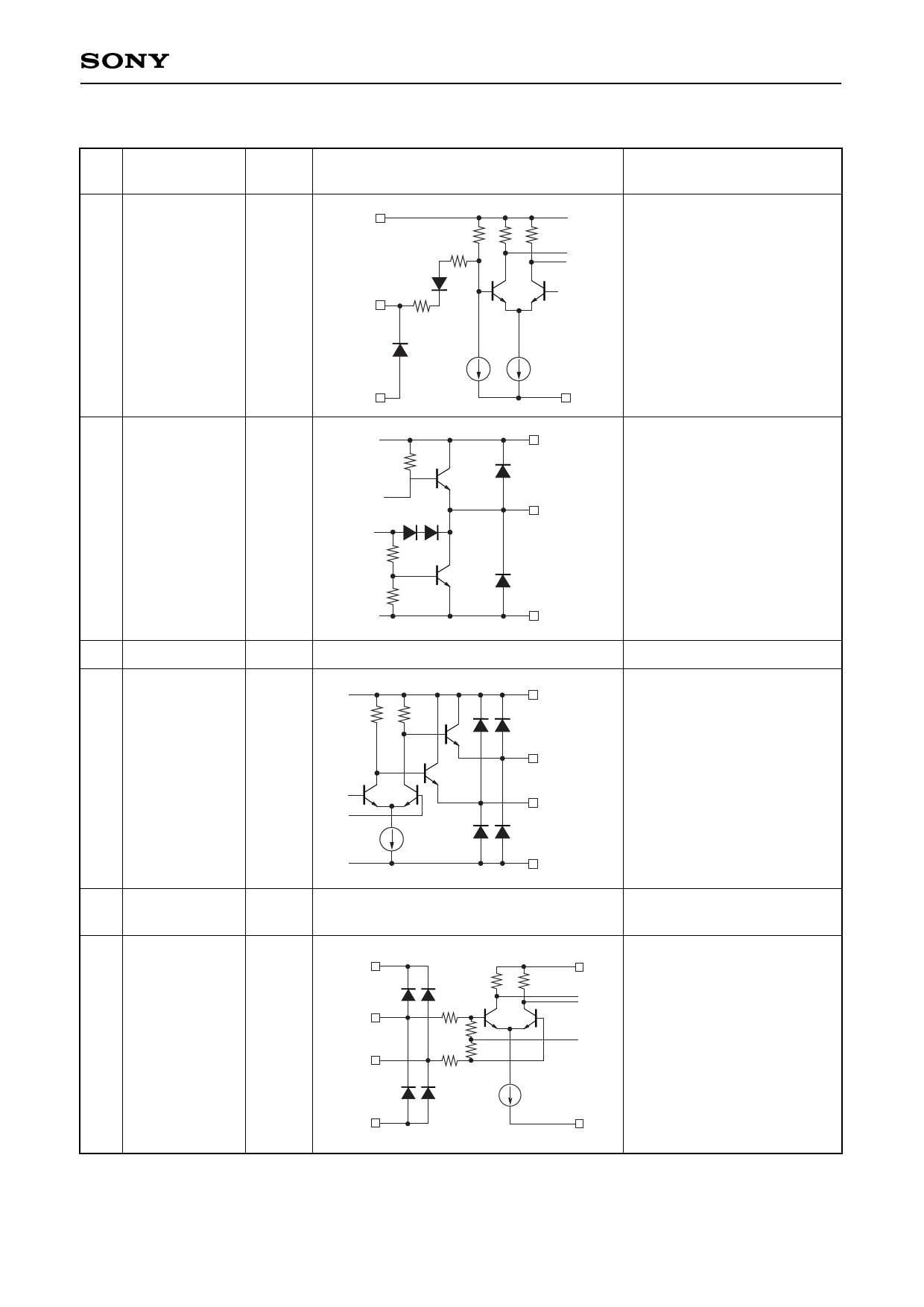
Pin Description
Pin
No.
Symbol
Type
VCCG
Equivalent circuit
1 REFCLK
Input
TTL
TTL_IN
Description
Reference clock.
This pin is used for the PLL
to take the frequency. Input
53.125MHz to this pin.
VEET
2 LKDT
Output
TTL
3 VEET
Ground
VEEG
VCCE
TTL_OUT
VEET
PLL lock detection signal
output.
Outputs high level when PLL
is locked to the serial data.
Outputs low level when
LKREFN is in the low level or
the serial data isn't locked to
the serial input data.
Ground for TTL I/O: 0V.
VCCE
4 DIAG_OUT
5 DIAG_OUTN
Output
ECL
6 VCCE
7 LOOP_IN
8 LOOP_INN
Power
supply
VCCE
Input
ECL
ECL_IN
ECL_INN
ECL_OUT
ECL_OUTN
Differential serial data output.
VEEE
Power supply for ECL l/O:
3.3V ± 5%.
VCCG
VCCE – 1.3V
Differential serial data input.
VEEE
–3–
VEEG
Share Link: 