TQ9303 Просмотр технического описания (PDF) - TriQuint Semiconductor
Номер в каталоге
Компоненты Описание
производитель
TQ9303 Datasheet PDF : 25 Pages
| |||
TQ9303
Table 10. AC Characteristics—Transmit (BTX) Timing (1)
Parameter
T9
T10
T11
T12
T13
Description
BTXCKN Pulse Width High
BTXCKIN Pulse Width Low
BTXCKIN Period
BTXD(0..9)-to-BTXCKOUT↑ setup time
BTXCKOUT↑-to-BTXD(0..9) hold time
Abs.Min. Rel.Min. Abs.Max. Rel.Max. Unit
3.2
0.4t
0.6t
ns
3.2
0.4t
0.6t
ns
8
t
t
ns
(2)
(2)
(2)
(2)
(2)
(2)
(2)
(2)
Notes: 1. “t” represents one (1) BTXCKIN period.
2. See Table 11, "Transmit (BTX) Timing Formulas,” below.
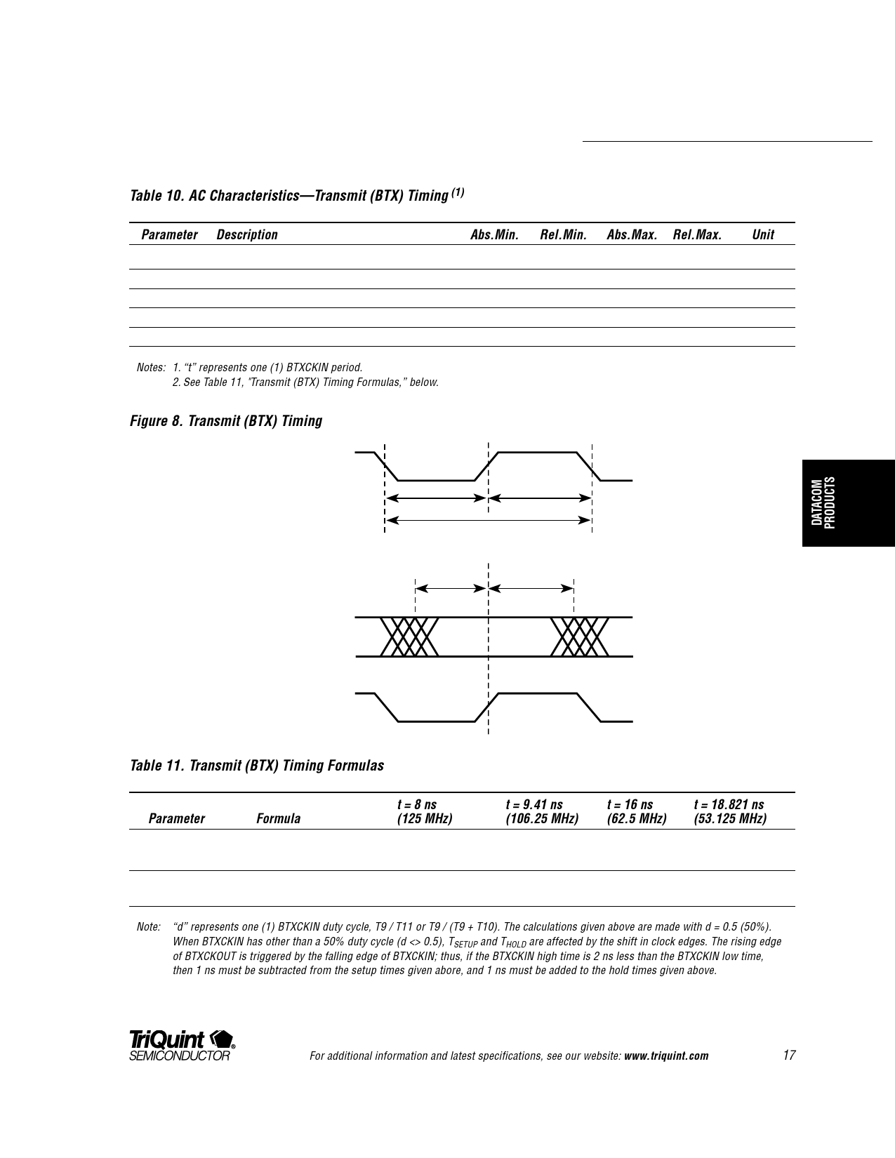
Figure 8. Transmit (BTX) Timing
BTXCKIN
T9
T10
T11
BTXD(0..9)
T12
T13
BTXCKOUT
Table 11. Transmit (BTX) Timing Formulas
Parameter
T12
T13
Formula
d * t – 1.94 ns
(1 – d) * t – 1.42 ns
t␣ =␣ 8␣ ns
(125␣ MHz)
2.06 ns
(1.8 ns min.)
2.58 ns
(3.4 ns min.)
t␣ =␣ 9.41␣ ns
(106.25␣ MHz)
2.76 ns
(2.5 ns min.)
3.28 ns
(2.1 ns min.)
t␣ =␣ 16␣ ns
(62.5␣ MHz)
6.06 ns
6.58 ns
t␣ =␣ 18.821␣ ns
(53.125␣ MHz)
7.47 ns
7.99 ns
Note:
“d” represents one (1) BTXCKIN duty cycle, T9␣ /␣ T11 or T9␣ /␣ (T9␣ +␣ T10). The calculations given above are made with d␣ =␣ 0.5␣ (50%).
When BTXCKIN has other than a 50% duty cycle (d <> 0.5), TSETUP and THOLD are affected by the shift in clock edges. The rising edge
of BTXCKOUT is triggered by the falling edge of BTXCKIN; thus, if the BTXCKIN high time is 2␣ ns less than the BTXCKIN low time,
then 1␣ ns must be subtracted from the setup times given abore, and 1␣ ns must be added to the hold times given above.
For additional information and latest specifications, see our website: www.triquint.com
17
Share Link: 