AD61009ARSZRL Просмотр технического описания (PDF) - Analog Devices
Номер в каталоге
Компоненты Описание
производитель
AD61009ARSZRL Datasheet PDF : 24 Pages
| |||
AD61009
The mixer’s output passes through both a low-pass filter and a
buffer, which provides an internal differential to single-ended
signal conversion with a bandwidth of approximately 45 MHz.
Its output at pin MXOP is in the form of a single-ended current.
This approach eliminates the 6 dB voltage loss of the usual series
termination by replacing it with shunt terminations at the both
the input and the output of the filter. The nominal conversion
gain is specified for operation into a total IF bandpass filter
(BPF) load of 165 Ω, that is, a 330 Ω filter, doubly-terminated
as shown in Figure 33. Note that these loads are connected to
bias point VMID, which is always at the midpoint of the supply
(that is, VP/2).
The conversion gain is measured between the mixer input and
the input of this filter, and varies between 1.5 dB and 26.5 dB
for a 165 Ω load impedance. Using filters of higher impedance,
the conversion gain can always be maintained at its specified
value or made even higher; for filters of lower impedance, of say
ZO, the conversion gain will be lowered by 10 log10(165/ZO).
Thus, the use of a 50 Ω filter will result in a conversion gain that
is 5.2 dB lower. Figure 3 shows filter matching networks and
Table I lists resistor values.
MXOP 8
VMID 9
R2
BPF
R1
100nF
1nF
10 IFHI
R3
11 IFLO
100nF
Figure 3. Suggested IF Filter Matching Network. The
Values of R1 and R2 Are Selected to Keep the Impedance
at Pin MXOP at 165 Ω
Table I. AD61009 Filter Termination Resistor Values for
Common IFs
Filter
Filter Termination Resistor
IF
Impedance Values1 for 24 dB of Mixer Gain
450 kHz
455 kHz
6.5 MHz
10.7 MHz
1500 Ω
1500 Ω
1000 Ω
330 Ω
R1
174 Ω
174 Ω
215 Ω
330 Ω
R2
1330 Ω
1330 Ω
787 Ω
0Ω
R3
1500 Ω
1500 Ω
1000 Ω
330 Ω
NOTE
1Resistor values were calculated such that R1 + R2 = ZFILTER and
R1ʈ (R2 + ZFILTER) = 165 Ω.
The maximum permissible signal level at MXOP is determined
by both voltage and current limitations. Using a 3 V supply and
VMID at 1.5 V, the maximum swing is about ± 1.3 V. To attain
a voltage swing of ± 1 V in the standard IF filter load of 165 Ω
load requires a peak drive current of about ± 6 mA, which is well
within the linear capability of the mixer. However, these upper
limits for voltage and current should not be confused with issues
related to the mixer gain, already discussed. In an operational
system, the AGC voltage will determine the mixer gain, and
hence the signal level at the IF input pin IFHI; it will always be
less than ± 56 mV (–15 dBm into 50 Ω), which is the limit of the
IF amplifier’s linear range.
IF Amplifier
Most of the gain in the AD61009 arises in the IF amplifier strip,
which comprises four stages. The first three are fully differential
and each has a gain span of 25 dB for the nominal AGC voltage
range. Thus, in conjunction with the mixer’s variable gain, the
total gain exceeds 90 dB. The final IF stage has a fixed gain of
20 dB, and it also provides differential to single-ended conversion.
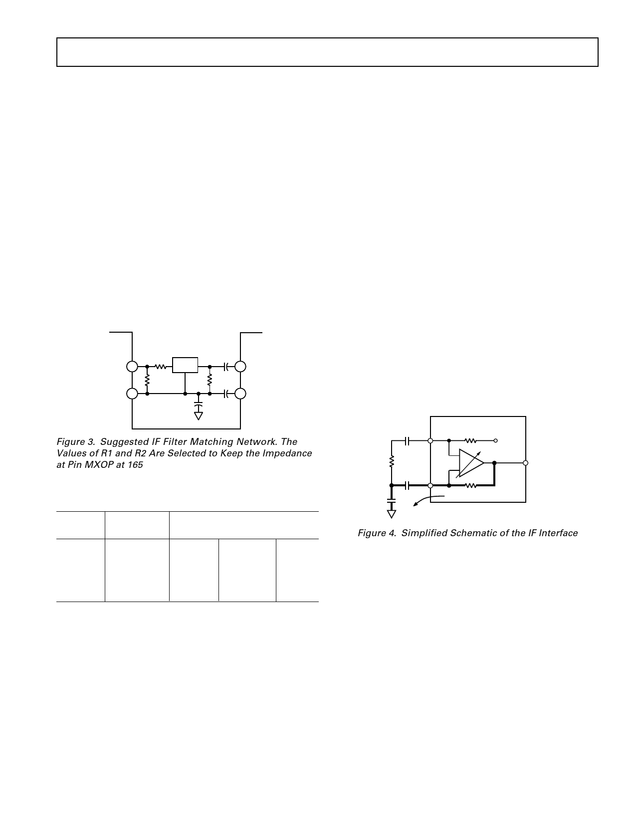
The IF input is differential, at IFHI (noninverting relative to the
output IFOP) and IFLO (inverting). Figure 4 shows a simplified
schematic of the IF interface. The offset voltage of this stage
would cause a large dc output error at high gain, so it is nulled by
a low-pass feedback path from the IF output, also shown in
TPC 25. Unlike the mixer output, the signal at IFOP is a low-
impedance single-sided voltage, centered at VP/2 by the dc
feedback loop. It may be loaded by a resistance as low as 50 Ω,
which will normally be connected to VMID.
AD61009
IFHI
10k⍀
VMID
IFOP
IFLO
10k⍀
OFFSET FEEDBACK
LOOP
Figure 4. Simplified Schematic of the IF Interface
The IF’s small-signal bandwidth is approximately 45 MHz from
IFHI and IFLO through IFOP. The peak output at IFOP is
± 560 mV at VP = 3 V and ± 400 mV at the minimum VP of
2.7 V. This allows some headroom at the demodulator inputs
(pin DMIP), which accept a maximum input of ± 150 mV for
IFs > 3 MHz and ± 75 mV for IFs ≤ 3 MHz (at IFs ≤ 3 MHz,
the drive to the demodulators must be reduced to avoid saturat-
ing the output amplifiers with higher order mixing products that
are no longer removed by the onboard low-pass filters).
REV. 0
–15–
Share Link: 