AD61009ARSZRL Просмотр технического описания (PDF) - Analog Devices
Номер в каталоге
Компоненты Описание
производитель
AD61009ARSZRL Datasheet PDF : 24 Pages
| |||
AD61009
15
10
5
0
0.5
1
1.5
2
2.5
GAIN VOLTAGE – Volts
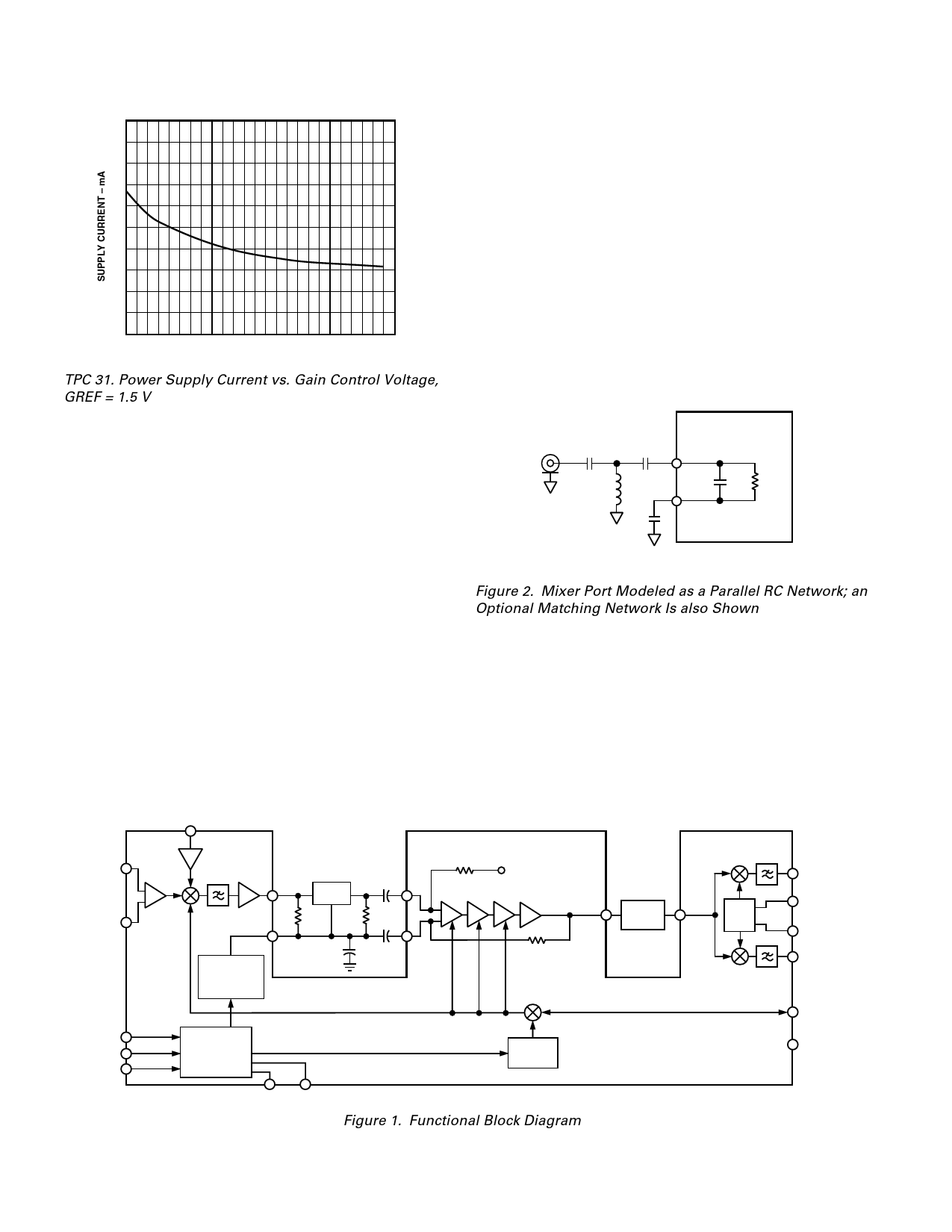
TPC 31. Power Supply Current vs. Gain Control Voltage,
GREF = 1.5 V
PRODUCT OVERVIEW
The AD61009 provides most of the active circuitry required to
realize a complete low power, single-conversion superheterodyne
receiver, or most of a double-conversion receiver, at input fre-
quencies up to 500 MHz, and with an IF of from 400 kHz to
12 MHz. The internal I/Q demodulators, and their associated
phase locked-loop, which can provide carrier recovery from
the IF, support a wide variety of modulation modes, including
n-PSK, n-QAM, and AM. A single positive supply voltage of
3 V is required (2.85 V minimum, 5.5 V maximum) at a typical
supply current of 8.5 mA at midgain. In the following discus-
sion, VP will be used to denote the power supply voltage, which
will be assumed to be 3 V.
Figure 1 shows the main sections of the AD61009. It consists of
a variable-gain UHF mixer and linear four-stage IF strip, which
together provide a voltage controlled gain range of more than
90 dB; followed by dual demodulators, each comprising a multi-
plier followed by a two-pole, 2 MHz low-pass filter; and driven
by a phase-locked loop providing the inphase and quadrature
clocks. A biasing system with CMOS compatible power-down
completes the AD61009.
Mixer
The UHF mixer is an improved Gilbert cell design, and can
operate from low frequencies (it is internally dc-coupled) up to
an RF input of 500 MHz. The dynamic range at the input of the
mixer is determined, at the upper end, by the maximum input
signal level of ± 56 mV between RFHI and RFLO up to which
the mixer remains linear, and, at the lower end, by the noise
level. It is customary to define the linearity of a mixer in terms
of the 1 dB gain-compression point and third-order intercept,
which for the AD61009 are –15 dBm and –8 dBm, respectively,
in a 50 Ω system.
The mixer’s RF input port is differential, that is, pin RFLO is
functionally identical to RFHI, and these nodes are internally
biased; we will generally assume that RFLO is decoupled to ac
ground. The RF port can be modeled as a parallel RC circuit as
shown in Figure 2.
C1
C2
L1
C3
AD61009
RFHI
RFLO
CIN RIN
C1, C2, L1: OPTIONAL MATCHING CIRCUIT
C3: COUPLES RFLO TO AC GROUND
Figure 2. Mixer Port Modeled as a Parallel RC Network; an
Optional Matching Network Is also Shown
The local oscillator (LO) input is internally biased at VP/2 via a
nominal 1000 Ω resistor internally connected from pin LOIP to
VMID. The LO interface includes a preamplifier which minimizes
the drive requirements, thus simplifying the oscillator design
and reducing LO leakage from the RF port. Internally, this
single-sided input is actually differential; the noninverting input
is referenced to pin VMID. The LO requires a single-sided drive
of ± 50 mV, or –16 dBm in a 50 Ω system.
LOIP
RFHI
RFLO
VPS1
VPS2
PRUP
MXOP
IFHI
BPF
MIDPOINT
BIAS
GENERATOR
VMID
IFLO
VMID
IFOP
BPF OR
LPF
DMIP
VQFO
BIAS
GENERATOR
PTAT
VOLTAGE
COM1 COM2
Figure 1. Functional Block Diagram
AD61009
IOUT
FDIN
FLTR
QOUT
GAIN
GREF
–14–
REV. 0
Share Link: 