VSC7130RC Просмотр технического описания (PDF) - Vitesse Semiconductor
Номер в каталоге
Компоненты Описание
производитель
VSC7130RC Datasheet PDF : 22 Pages
| |||
Data Sheet
VSC7130
VITESSE
SEMICONDUCTOR CORPORATION
Dual Repeater/Retimer
for Fibre Channel and Gigabit Ethernet
AC Characteristics (Over Recommended Operating Conditions)
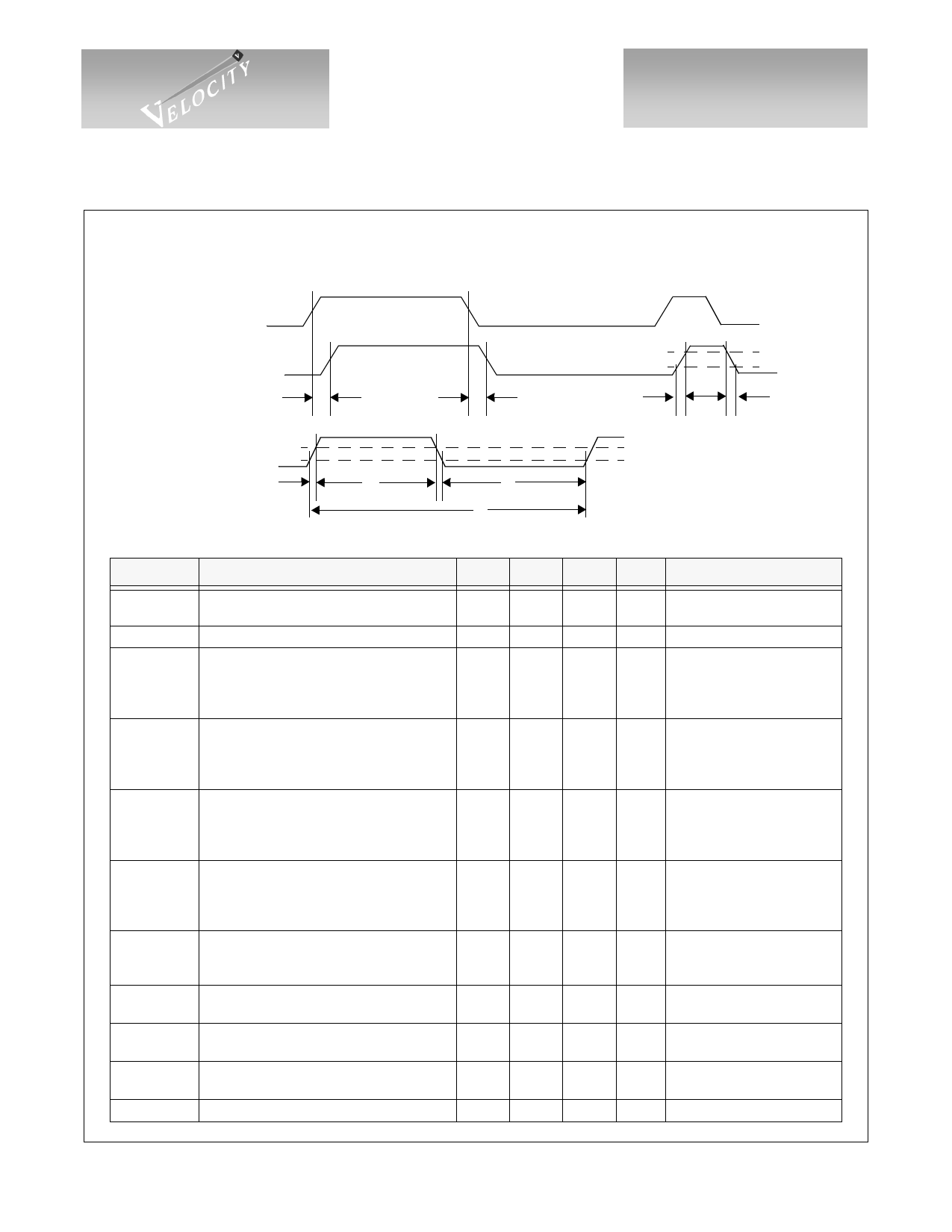
Figure 11: AC Timing Diagrams
RX0+/-
RX1+/-
SI1+/-
TX+/-
SO+/-
TP
TP
80%
20%
TS
TS
REFI
TT
TH
TT
TL
T
Table 5: AC Characteristics (Over recommended operating conditions)
VIH(MIN)
VIL(MAX)
Parameters
Description
Min Typ Max Units
Conditions
TP
Latency from any Serial Input to any Serial
Output
0.25
—
8.75
ns No Retimer in path
TS
TJ(RPTR)
Differential Output Rise/Fall time
Total data output jitter
[Repeater Mode]
—
— 300 ps Between 20% and 80%
Jitter Generation at TX/SO
—
—
192
ps
when driven by the CRU in
Repeater Mode. IEEE 802.3z
Clause 38.68
Jitter Generation at TX/SO
TDJ(RPTR)
Serial data output deterministic jitter (p-p)
[Repeater Mode]
—
—
80
ps
when driven by the CRU in
Repeater Mode. IEEE 802.3z
Clause 38.68
TJ(RTMR)
Total data output jitter [Retimer Mode]
Jitter Generation at TX/SO
—
—
192
ps
when driven by the CRU in
Retimer Mode. IEEE 802.3z
Clause 38.68
Jitter Generation at TX/SO
TDJ(RTMR)
Serial data output deterministic jitter (p-p)
[Retimer Mode]
—
—
80
ps
when driven by the CRU in
Retimer Mode. IEEE 802.3z
Clause 38.68
TJTOL
Jitter Tolerance at RX0/RX1/SI
Minimum Eye Opening for
0.24 —
—
UI proper operation as defined
in MJS 8.0.
TT
REFI input rise/fall times
F
REFI Frequency
—
—
1.5
ns
Between VIL(MAX) and
VIH(MIN)
105
52.5
—
126
63
MHz
HALF/FULL is LOW
HALF/FULL is HIGH
FO
Frequency Offset between incoming data
and REFI.
-200
— +200 ppm
DC
REFI Duty Cycle
30
70
% Measured at 1.5V
G52297-0, Rev 4.0
04/02/01
© VITESSE SEMICONDUCTOR CORPORATION • 741 Calle Plano • Camarillo, CA 93012
Tel: (800) VITESSE • FAX: (805) 987-5896 • Email: prodinfo@vitesse.com
Internet: www.vitesse.com
Page 15
Share Link: 