VT82C586B Просмотр технического описания (PDF) - Unspecified
Номер в каталоге
Компоненты Описание
производитель
VT82C586B Datasheet PDF : 69 Pages
| |||
9,$7HFKQRORJLHV,QF
VT82C586B
REGISTERS
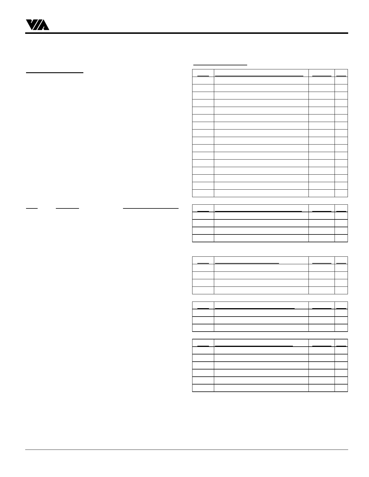
Register Overview
The following tables summarize the configuration and I/O
registers of the VT82C586B. These tables also document the
power-on default value (“Default”) and access type (“Acc”) for
each register. Access type definitions used are RW
(Read/Write), RO (Read/Only), “—” for reserved / used
(essentially the same as RO), and RWC (or just WC) (Read /
Write 1’s to Clear individual bits). Registers indicated as RW
may have some read/only bits that always read back a fixed
value (usually 0 if unused); registers designated as RWC or
WC may have some read-only or read write bits (see individual
register descriptions for details).
Detailed register descriptions are provided in the following
section of this document. All offset and default values are
shown in hexadecimal unless otherwise indicated
Table 2. System I/O Map
Port
00-1F
Function
Actual Port Decoding
Master DMA Controller 0000 0000 000x nnnn
20-3F
Master Interrupt Controller 0000 0000 001x xxxn
40-5F Timer / Counter
0000 0000 010x xxnn
60-6F
(60h)
(61h)
(64h)
Keyboard Controller
0000 0000 0110 xnxn
KBC Data
0000 0000 0110 x0x0
Misc Functions & Spkr Ctrl 0000 0000 0110 xxx1
KBC Command / Status 0000 0000 0110 x1x0
70-77
78-7F
RTC/CMOS/NMI-Disable 0000 0000 0111 0nnn
-available for system use- 0000 0000 0111 1xxx
80
81-8F
-reserved- (debug port)
DMA Page Registers
0000 0000 1000 0000
0000 0000 1000 nnnn
90-91
92
93-9F
-available for system use- 0000 0000 1001 000x
System Control
0000 0000 1001 0010
-available for system use- 0000 0000 1001 nnnn
A0-BF Slave Interrupt Controller 0000 0000 101x xxxn
C0-DF Slave DMA Controller 0000 0000 110n nnnx
E0-FF -available for system use- 0000 0000 111x xxxx
100-CF7 -available for system use-
CF8-CFB PCI Configuration Address 0000 1100 1111 10xx
CFC-CFF PCI Configuration Data 0000 1100 1111 11xx
D00-FFFF -available for system use-
Table 3. Registers
Legacy I/O Registers
Port Master DMA Controller Registers
00 Channel 0 Base & Current Address
01 Channel 0 Base & Current Count
02 Channel 1 Base & Current Address
03 Channel 1 Base & Current Count
04 Channel 2 Base & Current Address
05 Channel 2 Base & Current Count
06 Channel 3 Base & Current Address
07 Channel 3 Base & Current Count
08 Status / Command
09 Write Request
0A Write Single Mask
0B Write Mode
0C Clear Byte Pointer FF
0D Master Clear
0E Clear Mask
0F Read / Write Mask
Default Acc
RW
RW
RW
RW
RW
RW
RW
RW
RW
WO
WO
WO
WO
WO
WO
RW
Port Master Interrupt Controller Regs
20 Master Interrupt Control
21 Master Interrupt Mask
20 Master Interrupt Control Shadow
21 Master Interrupt Mask Shadow
* RW if shadow registers are disabled
Default Acc
—*
—*
— RW
— RW
Port Timer/Counter Registers
40 Timer / Counter 0 Count
41 Timer / Counter 1 Count
42 Timer / Counter 2 Count
43 Timer / Counter Control
Default Acc
RW
RW
RW
WO
Port Keyboard Controller Registers
60 Keyboard Controller Data
61 Misc Functions & Speaker Control
64 Keyboard Ctrlr Command / Status
Default Acc
RW
RW
RW
Port CMOS / RTC / NMI Registers
Default Acc
70 CMOS Memory Address & NMI Disa
WO
71 CMOS Memory Data (128 bytes)
RW
72 CMOS Memory Address
RW
73 CMOS Memory Data (256 bytes)
RW
74 CMOS Memory Address
RW
75 CMOS Memory Data (256 bytes)
RW
NMI Disable is port 70h (CMOS Memory Address) bit-7.
RTC control occurs via specific CMOS data locations (0-0Dh).
Ports 72-73 may be used to access all 256 locations of CMOS.
Ports 74-75 may be used to access CMOS if the internal RTC is
disabled.
Revision 1.0 May 13, 1997
-14-
Register Overview
Share Link: 