UAA3580HN Просмотр технического описания (PDF) - Philips Electronics
Номер в каталоге
Компоненты Описание
производитель
UAA3580HN
Philips Electronics

UAA3580HN Datasheet PDF : 24 Pages
| |||
Philips Semiconductors
Wideband code division multiple access
frequency division duplex zero IF receiver
Objective specification
UAA3580
9.3 RF PLL synthesizer
The RF fractional-N synthesizer is set via the 3-wire bus
with the FRAC and CH chains. CH sets the integer divider
ratio and FRAC the fractional divider ratio. They both
provide the LO frequency in accordance with the following
equation:
fRFLO
=
fref
×
N----2-R----X-
+
Kfrac(RX)
Where
Kfrac(RX)
=
-2--1-2---2
×
KR
X
+
12--
Where KRX is the integer value of FRAC[21:0], NRX is the
integer value of CH[8:0] and fref is the external frequency
reference applied to pin REFIN.
Example: to obtain a fRFLO frequency of 2.14 GHz with an
error less than ∆fPLL NRX must be set to 164 and Kfrac(RX)
to 1290555 if the reference frequency is 26 MHz. It should
be noted that some particular frequencies can be obtained
in two ways; NRX = x and Kfrac(RX) = 0.25 provides the
same frequency as NRX = x − 1 and Kfrac(RX) = 0.75
9.4 Clock PLL synthesizer
9.4.1 AFC MODE
The clock PLL is based on the SD fractional-N synthesizer
that allows to derive the UMTS system clock including AFC
from a non-corrected external 26 MHz only GMS
reference. The clock PLL frequency with the AFC
correction word is given by the following equation:
fCLKPLL
=
fr
ef
×
-9----+-----K-2----A---F---C--
Where KAFC = 25----31---12-- + -A--2--F-2---1C---
AFC represents the integer value of AFC[11:0] and fref is
the external reference frequency applied to pin REFIN.
9.4.2 CLOCK PLL MODES
The clock PLL synthesizer is controlled by bits CLKon and
CLKoff. At power-up the clock PLL synthesizer is
automatically on when pin RXCEN is set HIGH. The
control, done with CLKon, will be reset at the rising edge
of RXCEN. For application which do not require the UMTS
clock system, the clock PLL can be powered-down with bit
CLKoff set to logic 1.
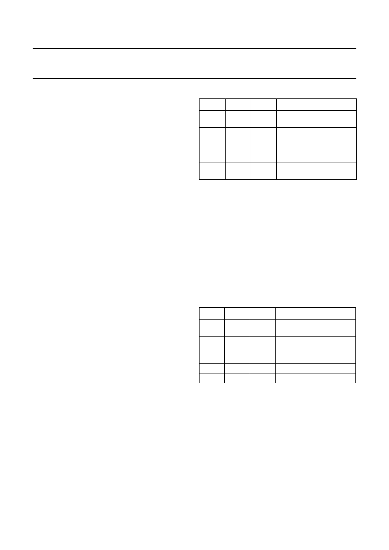
Table 4 Clock mode
RXCEN CLKon CLKoff
DESCRIPTION
1
1
0 CLKPLL synthesizer
enabled (default)
0
1
0 CLKPLL synthesizer
disabled; note 1
1
0
X(4)
X(4)
0 CLKPLL synthesizer
disabled; note 2
1 CLKPLL synthesizer
disabled; note 3
Notes
1. Hard power-down of the clock PLL done with RXCEN.
2. Power-down achieved via the 3-wire bus, reset by
RXCEN.
3. Power-down achieved via the 3-wire bus, no effect by
RXCEN in this mode. This mode will be reset if VDDD
is not maintained.
4. X = don’t care.
9.4.3 CLOCK PLL OUTPUT DIVIDER
The clock PLL output divider ratio is set in accordance with
Table 5.
Table 5 Clock mode; note 1
CLKoff CLK1
1
X
0
0
0
0
0
1
0
1
CLK0
X
0
1
0
1
DESCRIPTION
UMTSCLKO output
disabled
clock divider ratio set to
default
clock divider ratio set to 2
clock divider ratio set to 4
clock divider ratio set to 8
Note
1. X = don’t care.
2002 Oct 30
11
Share Link: