SST37VF010-70-3C-NHE Просмотр технического описания (PDF) - Silicon Storage Technology
Номер в каталоге
Компоненты Описание
производитель
SST37VF010-70-3C-NHE
Silicon Storage Technology

SST37VF010-70-3C-NHE Datasheet PDF : 18 Pages
| |||
512 Kbit / 1 Mbit / 2 Mbit / 4 Mbit Many-Time Programmable Flash
SST37VF512 / SST37VF010 / SST37VF020 / SST37VF040
Data Sheet
Byte-Program Operation
The SST37VF512/010/020/040 are programmed by using
an external programmer. The programming mode is acti-
vated by asserting 11.4-12V on OE# pin and VIL on CE#
pin. The device is programmed using a single pulse (WE#
pin low) of 15 µs per byte. Using the MTP programming
algorithm, the Byte-Program process continues byte-by-
byte until the entire chip has been programmed. Refer to
Figure 11 for the flowchart and Figure 7 for the timing dia-
gram.
Chip-Erase Operation
The only way to change a data from a “0” to “1” is by
electrical erase that changes every bit in the device to
“1”. The SST37VF512/010/020/040 use an electrical
Chip-Erase operation. The entire chip can be erased
in 100 ms (WE# pin low). In order to activate erase
mode, the 11.4-12V is applied to OE# and A9 pins
while CE# is low. All other address and data pins are
“don’t care”. The falling edge of WE# will start the
Chip-Erase operation. Once the chip has been erased,
all bytes must be verified for FFH. Refer to Figure 10
for the flowchart and Figure 6 for the timing diagram.
Product Identification Mode
The Product Identification mode identifies the devices as
SST37VF512, SST37VF010, SST37VF020, and
SST37VF040 and manufacturer as SST. This mode may
be accessed by the hardware method. To activate this
mode, the programming equipment must force VH (11.4-
12V) on address A9. Two identifier bytes may then be
sequenced from the device outputs by toggling address
line A0. For details, see Table 3 for hardware operation.
TABLE 1: Product Identification
Manufacturer’s ID
Address
0000H
Device ID
SST37VF512
SST37VF010
SST37VF020
SST37VF040
0001H
0001H
0001H
0001H
Data
BFH
C4H
C5H
C6H
C2H
T1.2 1151
Design Considerations
The SST37VF512/010/020/040 should have a 0.1 µF
ceramic high frequency, low inductance capacitor con-
nected between VDD and GND. This capacitor should be
placed as close to the package terminals as possible.
OE# and A9 must remain stable at VH for the entire dura-
tion of an Erase operation. OE# must remain stable at VH
for the entire duration of the Program operation.
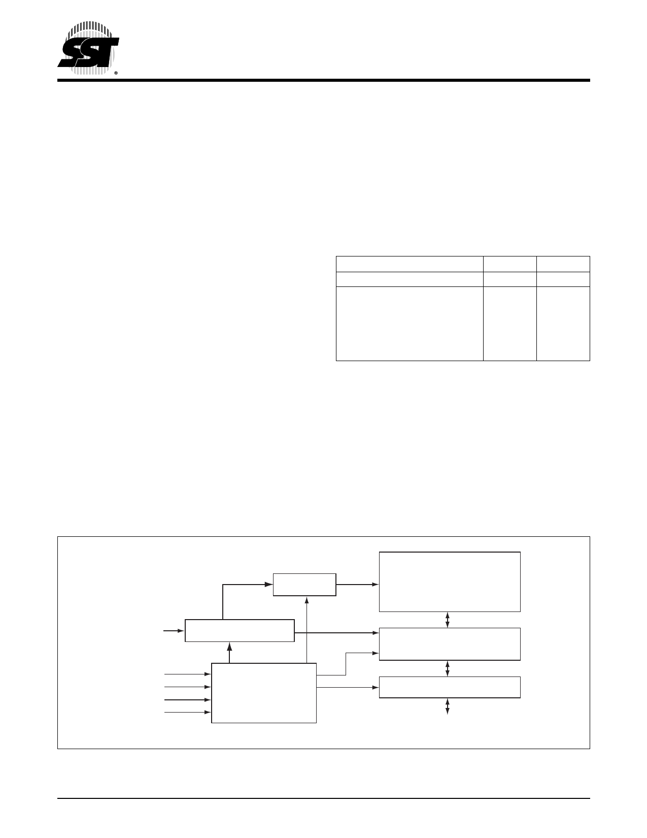
X-Decoder
Memory Address
Address Buffer
CE#
OE#
A9
WE#
Control Logic
FIGURE 1: Functional Block Diagram
©2006 Silicon Storage Technology, Inc.
2
SuperFlash
Memory
Y-Decoder
I/O Buffers
DQ7 - DQ0
1151 B1.1
S71151-07-000
8/06
Share Link: