SC508 –ü—Ä–æ—Å–º–æ—Ç—Ä —Ç–µ—Ö–Ω–∏—á–µ—Å–∫–æ–≥–æ –æ–ø–∏—Å–∞–Ω–∏—è (PDF) - Semtech Corporation
–ù–æ–º–µ—Ä –≤ –∫–∞—Ç–∞–ª–æ–≥–µ
–ö–æ–º–ø–æ–Ω–µ–Ω—Ç—ã –û–ø–∏—Å–∞–Ω–∏–µ
–ø—Ä–æ–∏–∑–≤–æ–¥–∏—Ç–µ–ª—å
SC508 Datasheet PDF : 32 Pages
| |||
SC508/SC508A
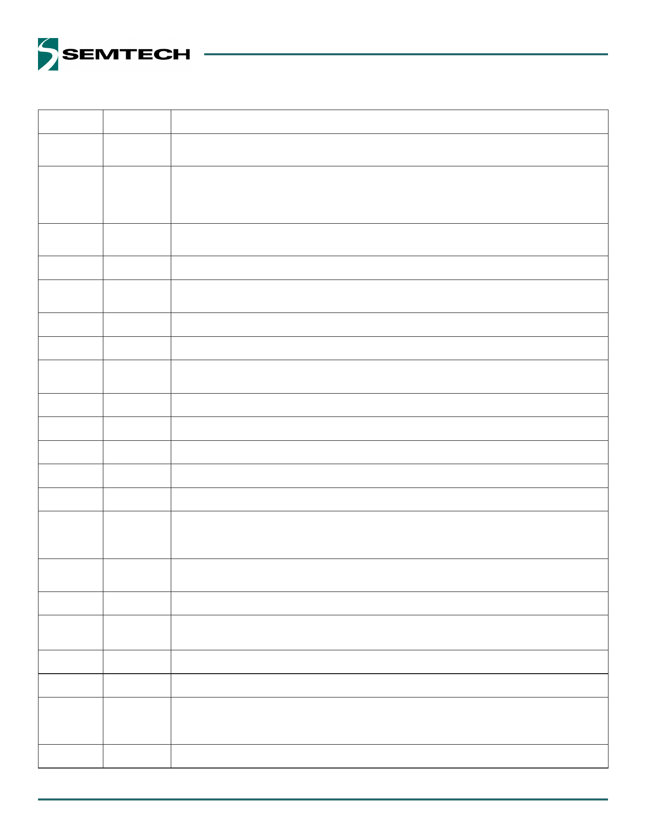
Pin Descriptions
Pin #
1
2
3
4
5
6
7
8
9
10
11
12
13
14
15
16
17
18
19
20
PAD
Pin Name Pin Function
FB
Feedback input for switching regulator — connect to an external resistor divider from output — used to pro-
gram the output voltage.
VOUT
Switcher output voltage sense pin — also the input to the internal switch-over MOSFET between VOUT and
VLDO. The voltage at this pin must not exceed the VDDA pin. For output voltages up to 5V connect this pin
directly to the switcher output. For output voltages exceeding 5V connect this pin to the switcher output
through a resistor divider.
VDDA
Supply input for internal analog circuits — connect to external 5V supply or connect to VLDO — also the
sense input for VDDA Under Voltage Lockout (VDDA UVLO).
VLDO
Output of the 5V LDO — The voltage at this pin must not exceed the voltage at the VDDA pin.
VIN
Input supply voltage — connect to the same supply used for the high-side MOSFET. Connect a 100nF capaci-
tor from this pin to AGND to filter high frequency noise.
SS
Soft-Start — connect tan external capacitor to AGND to program the soft start and automatic recovery time.
NC
No Connection
BST
Bootstrap pin — connect a 100nF minimum capacitor and series resistor from BST to LX to develop the float-
ing voltage for the high-side gate drive. A 3.3 ohm resistor is recommended.
DH
High-side gate drive output
LX
Switching (phase) node
PGND
Power ground for the DL and DH drivers and the low-side external MOSFET.
DL
Low-side gate drive output
VDDP
5V supply input for the DH and DL gate drives — connect to the same 5V supply used for VDDA.
PSV
PGOOD
ILIM
Power-save programming input — connect a resistor to AGND to set a minimum (ultrasonic) power-save fre-
quency — float pin to select power-save with no minimum frequency — pull up to VDDA to disable power-
save and select forced continuous mode.
Open-drain Power Good indicator — high impedance indicates the switching regulator output is good. An
external pull-up resistor is required.
Current limit sense pin — used to program the current limit by connecting a resistor from ILIM to LX.
Enable input for switching regulator — logic low disables the switching regulator — logic high enables the
EN
switching regulator.
AGND
Analog ground
TON
ON time programming input — set the on-time by connecting through a resistor to AGND.
ENL
AGND
Enable input for the LDO and VIN UVLO input for the switching regulator — connect ENL to AGND to disable
the LDO — drive to logic high (>1.7V) to enable the LDO and inhibit VIN UVLO — connect to resistor divider
from VIN to AGND to program the VIN UVLO threshold.
Analog ground
11
Share Link: 