RF3158 Просмотр технического описания (PDF) - RF Micro Devices
Номер в каталоге
Компоненты Описание
производитель
RF3158 Datasheet PDF : 26 Pages
| |||
RF3158
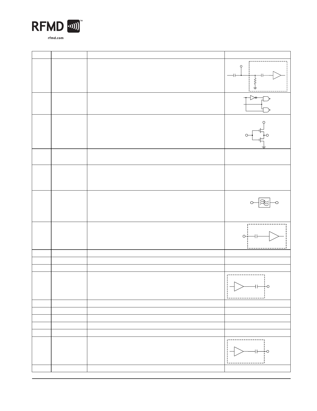
Pin Function Description
Interface Schematic
1
HB_RFIN RF input to the high-band PA. There is a 100Ω shunt resistor, before the
HB_RFIN RF3158 PAM
DC block inside the part, which sets the input impedance for the HB PA.
External
When connected to a DC coupled transceiver, an external DC blocking
DC Block
DC Block
capacitor is required.
100 Ω
2
BAND_SEL Digital input enables either the low band or high band amplifier die within BAND SEL
the module. A logic low selects Low Band (GSM850/EGSM900), a logic
high selects High Band (DCS1800/PCS1900). This pin is a high impedance
TX EN
CMOS input with no pull-up or pull-down resistors.
GSM CTRL
DCS CTRL
3
TX_EN
Digital input enables or disables the internal circuitry. When disabled, the
module is in the OFF state and draws virtually zero current. This pin is a
high impedance CMOS input with no pull-up or pull-down resistors.
VBATT
TX EN
TX ON
4
VBATT
Main DC power supply for all circuitry in the RF3158. Traces to this pin will
have high current pulses during operation so proper decoupling and rout-
ing to handle this should be observed.
5
VMODE
Digital input which internally adjusts settings to optimize amplifier perfor-
mance for saturated or linear mode. A logic low selects saturated mode for
GMSK modulation. A logic high selects linear mode for 8PSK modulation.
This pin is a high impedance CMOS input with no pull-up or pull-down resis-
tors.
6
VRAMP
In GMSK mode, the voltage on this pin controls the output power by varying
the regulated collector voltage on the amplifiers. In EDGE mode, the volt-
300 kHz
age on this pin varies the regulated base bias of the amplifiers. An internal
VRAMP
300kHz filter reduces switching ORFS resulting from transitions between
DAC steps. Most systems will have no need for external VRAMP filtering. This
pin provides an impedance of approximately 60kΩ.
7
LB_RFIN RF input to the low-band PA. It is DC-blocked within the part.
DC Block
LB_RFIN
8
GND
Ground.
10
GND
Ground.
11
GND
Ground.
12
LB_RFOUT RF output from the low-band PA. It is DC-blocked within the part.
RF3158 PAM
DC Block
LB_RFOUT
13
GND
Ground.
14
GND
Ground.
15
GND
Ground.
16
GND
Ground.
17
GND
Ground.
18
HB_RFOUT RF output from the high-band PA. It is DC-blocked within the part.
RF3158 PAM
DC Block
HB_RFOUT
19
GND
Ground.
RF3158 PAM
Rev A2 DS070615
7628 Thorndike Road, Greensboro, NC 27409-9421 · For sales or technical
support, contact RFMD at (+1) 336-678-5570 or sales-support@rfmd.com.
11 of 26
Share Link: 