RF3158 Просмотр технического описания (PDF) - RF Micro Devices
Номер в каталоге
Компоненты Описание
производитель
RF3158 Datasheet PDF : 26 Pages
| |||
RF3158
GSM applications typically require an input RF drive that is 3dB to 4dB higher than the 1dB compression point. GSM mode
involves GMSK modulation, which is a constant envelope modulation and is not sensitive to amplitude non-linearities caused
by the PA. Since the useful data in the GMSK modulation is entirely included in the phase, the amplifier may be operated in
saturated mode (deep class AB) for optimum efficiency. Saturated output power for the RF3158 is controlled by the voltage on
the VRAMP pin.
Linear EDGE applications require a linear power amplifier to transfer 8PSK modulation with minimal distortion. Since an 8PSK
signal has information encoded in both amplitude and phase, the use of a saturated PA is not trivial and requires a more com-
plex system. The traditional way to design a transmitter that is required to convey both phase and amplitude modulation is
through the use of a linear power amplifier (Class A). In RF3158, the bias is held at a constant level such that the device is
operating in linear region, and the output RF level is directly proportional to the input RF level. The RF3158 is used as a linear
amplifier by fixing the voltage on the VRAMP pin and reducing the input power to the PA such that the device enters a linear
operational region. Output power is controlled by applying the proper amplitude signal to the RFIN Pin. The voltage on the
VRAMP pin controls bias current and can be fixed at various levels to optimize current consumption for the desired output power
range.
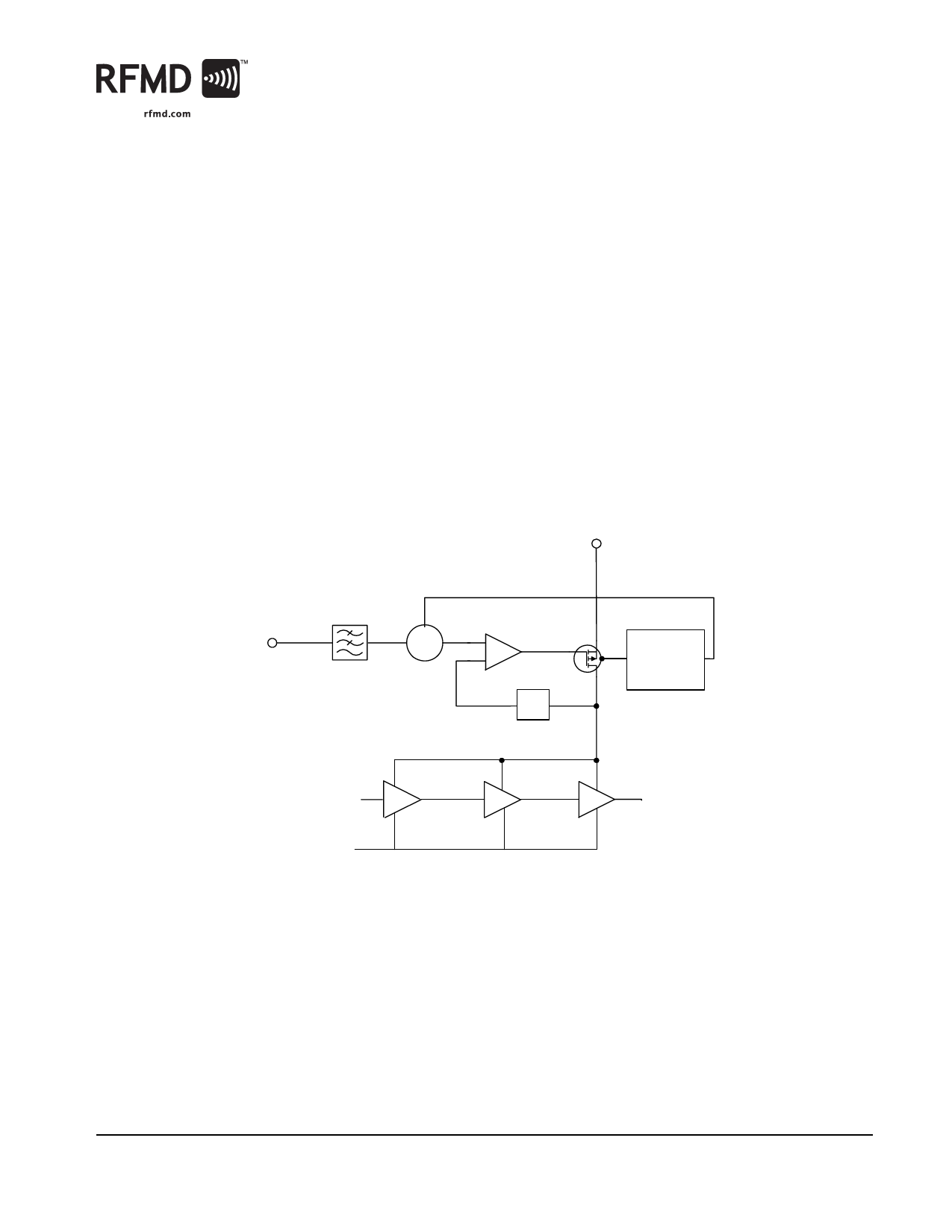
GSM (Saturated) Mode
In GSM mode, RF3158 operates as a traditional PowerStar® module. The incorporated control loop regulates the collector volt-
age of the amplifiers while the stages are held at a constant bias. The basic circuit diagram is shown in Figure 2.
VBATT
V RAMP
-
+
3 dB BW
300 kHz
-
+
H(s)
Saturation
Detector
VCC
RF IN
RF OUT
TX ENABLE
Figure 2. RF3158 Basic Circuit Diagram
By regulating the collector voltage (VCC), the stages are held in saturation across all power levels. As VCC is decreased, output
power decreases as described by Equation 1. The equation shows that load impedance affects output power, but to a lesser
degree than VCC supply variations. Since the RF3158 regulates VCC, the dominant cause of power variation is eliminated.
POUTdBm
=
10 ⋅ log -(--2----⋅---V----C----C----–-----V----S---A---T---)--2-
8 ⋅ Rl ⋅ 10–3
(Eq. 1)
Rev A2 DS070615
7628 Thorndike Road, Greensboro, NC 27409-9421 · For sales or technical
support, contact RFMD at (+1) 336-678-5570 or sales-support@rfmd.com.
15 of 26
Share Link: 