PCA9512B(2011) Просмотр технического описания (PDF) - NXP Semiconductors.
Номер в каталоге
Компоненты Описание
производитель
PCA9512B Datasheet PDF : 24 Pages
| |||
NXP Semiconductors
PCA9512A; PCA9512B
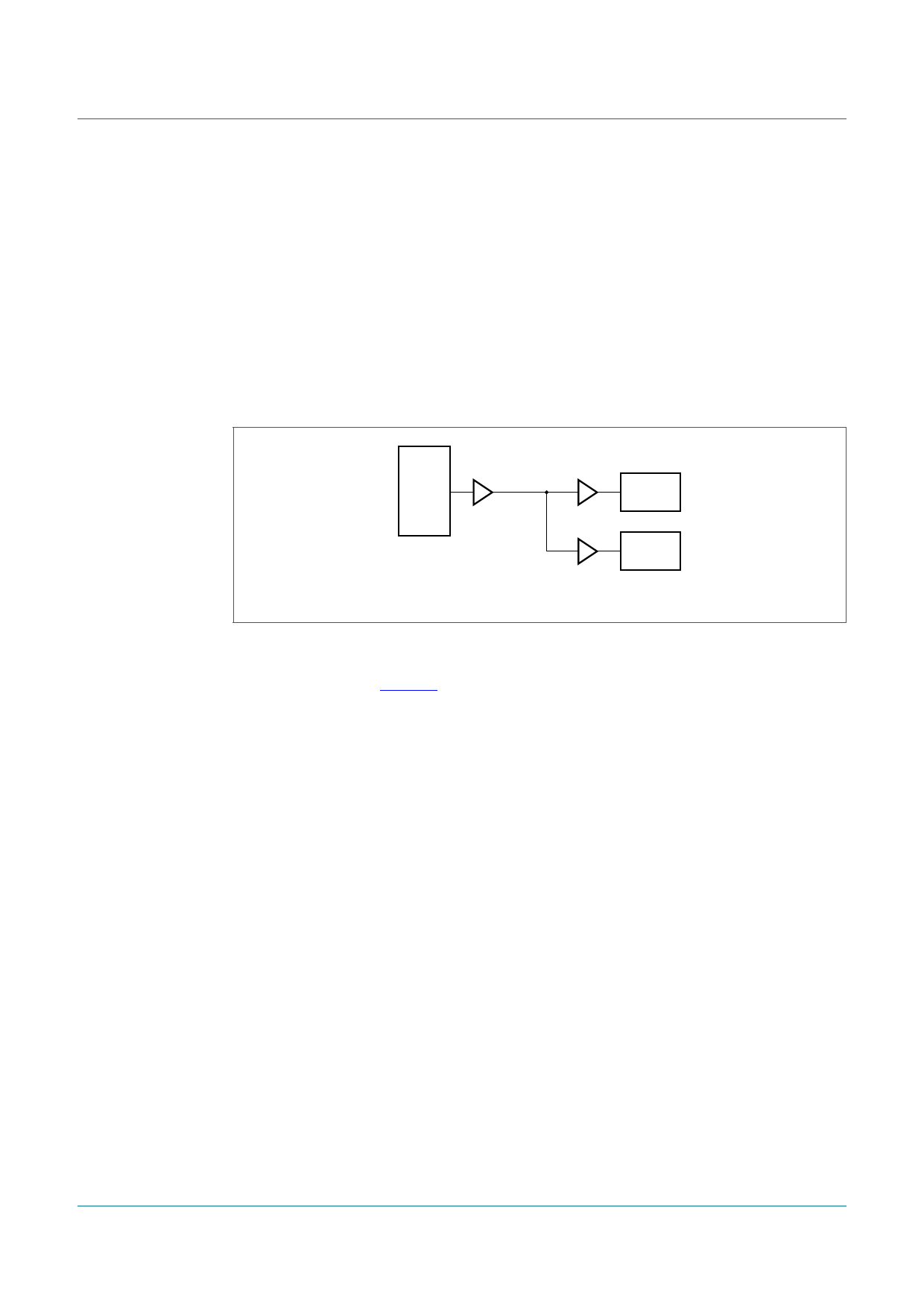
Level shifting hot swappable I2C-bus and SMBus bus buffer
slew rate is slow enough that the output catches up it will still lag the falling voltage of the
input by the offset voltage. The maximum tPHL occurs when the input is driven LOW with
zero delay and the output is still limited by its turn-on delay and the falling edge slew rate.
The output falling edge slew rate is a function of the internal maximum slew rate which is
a function of temperature, VCC or VCC2 and process, as well as the load current and the
load capacitance.
8.5 Rise time accelerators
During positive bus transactions, a 2 mA current source is switched on to quickly slew the
SDA and SCL lines HIGH once the input level of 0.6 V for the PCA9512A/B is exceeded.
The rising edge rate should be at least 1.25 V/μs to guarantee turn on of the accelerators.
The built-in ΔV/Δt rise time accelerators on all SDA and SCL lines requires the bus pull-up
voltage and respective supply voltage (VCC or VCC2) to be the same. The built-in ΔV/Δt
rise time accelerators can be disabled through the ACC pin for lightly loaded systems.
8.6 ACC boost current enable
Users having lightly loaded systems may wish to disable the rise time accelerators.
Driving this pin to ground turns off the rise time accelerators on all four SDAn and SCLn
pins. Driving this pin to the VCC2 voltage enables normal operation of the rise time
accelerators.
8.7 Resistor pull-up value selection
The system pull-up resistors must be strong enough to provide a positive slew rate of
1.25 V/μs on the SDAn and SCLn pins, in order to activate the boost pull-up currents
during rising edges. Choose maximum resistor value using the formula given in
Equation 1:
RP
U
≤
800
×
103
⎛
⎝
V----C----C---(--m---C-i-n---)---–----0---.--6-⎠⎞
(1)
where RPU is the pull-up resistor value in Ω, VCC(min) is the minimum VCC voltage in volts,
and C is the equivalent bus capacitance in picofarads.
In addition, regardless of the bus capacitance, always choose RPU ≤ 65.7 kΩ for
VCC = 5.5 V maximum, RPU ≤ 45 kΩ for VCC = 3.6 V maximum. The start-up circuitry
requires logic HIGH voltages on SDAOUT and SCLOUT to connect the backplane to the
card, and these pull-up values are needed to overcome the precharge voltage. See the
curves in Figure 5 and Figure 6 for guidance in resistor pull-up selection.
PCA9512A_PCA9512B
Product data sheet
All information provided in this document is subject to legal disclaimers.
Rev. 5 — 5 January 2011
© NXP B.V. 2011. All rights reserved.
7 of 24
Share Link: 