NCV8570 Просмотр технического описания (PDF) - ON Semiconductor
Номер в каталоге
Компоненты Описание
производитель
NCV8570 Datasheet PDF : 12 Pages
| |||
NCV8570
APPLICATION INFORMATION
General
The NCV8570 is a 200 mA (current limited) linear
regulator with a logic input for on/off control for the high
speed turn−off output voltage.
Access to the major contributor of noise within the
integrated circuit is provided as the focus for noise reduction
within the linear regulator system.
Power Up/Down
During power up, the NCV8570 maintains a high
impedance output (Vout) until sufficient voltage is present on
Vin to power the internal bandgap reference voltage. When
sufficient voltage is supplied (approx 1.2 V), Vout will start
to turn on (assume CE shorted to Vin), linearly increasing
until the output regulation voltage has been reached.
Active discharge circuitry has been implemented to insure
a fast turn off time. Then CE goes low, the active discharge
transistor turns on creating a fast discharge of the output
voltage. Power to drive this circuitry is drawn from the
output node. This is to maintain the lowest quiescent current
when in the sleep mode (VCE = 0.4 V). This circuitry
subsequently turns off when the output voltage discharges.
CE (chip enable)
The enable function is controller by the logic pin CE. The
voltage threshold of this pin is set between 0.4 V and 1.2 V.
A voltage lower than 0.4 V guarantees the device is off. A
voltage higher than 1.2 V guarantees the device is on. The
NCV8570 enters a sleep mode when in the off state drawing
less than 1 mA of quiescent current.
The device can be used as a simple regulator without use
of the chip enable feature by tying the CE pin to the Vin pin.
Current Limit
Output Current is internally limited within the IC to a
minimum of 200 mA. The design is set to a higher value to
allow for variation in processing and the temperature
coefficient of the parameter. The NCV8570 will source this
amount of current measured with a voltage 100 mV lower
than the typical operating output voltage.
The specification for short circuit current limit (@ Vout =
0 V) is specified at 320 mA (typ). There is no additional
circuitry to lower the current limit at low output voltages.
This number is provided for informational purposes only.
Output Capacitor
The NCV8570 has been designed to work with low ESR
ceramic capacitors. There is no ESR lower limit for stability
for the recommended 1 mF output capacitor. Stable region
for Output capacitor ESR vs Output Current is shown in
Figure 23.
Typical characteristics were measured with Murata
ceramic capacitors. GRM219R71E105K (1 mF, 25 V, X7R,
0805) and GRM21BR71A106K (10 mF, 10 V, X7R, 0805).
Output Noise
The main contributor for noise present on the output pin
Vout is the reference voltage node. This is because any noise
which is generated at this node will be subsequently
amplified through the error amplifier and the PMOS pass
device. Access to the reference voltage node is supplied
directly through the Cnoise pin. Noise can be reduced from
a typical value of 20 mVrms by using 10 nF to 15 mVrms by
using a 100 nF from the Cnoise pin to ground.
A bypass capacitor is recommended for good noise
performance and better load transient response.
Thermal Shutdown
When the die temperature exceeds the Thermal Shutdown
threshold, a Thermal Shutdown (TSD) event is detected and
the output (Vout) is turned off. There is no effect from the
active discharge circuitry. The IC will remain in this state
until the die temperature moves below the shutdown
threshold (150C typical) minus the hysteresis factor (20C
typical).
This feature provides protection from a catastrophic
device failure due to accidental overheating. It is not
intended to be used as a substitute for proper heat sinking.
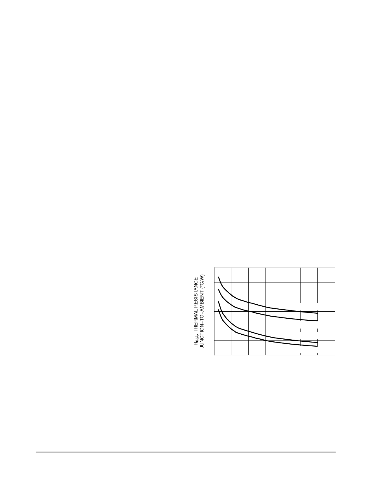
The maximum device power dissipation can be calculated
by:
PD
+
TJ * TA
RqJA
Thermal resistance value versus copper area and package is
shown in Figure 24.
380
330
280
TSOP−5 (1 oz)
230
180
TSOP−5 (2 oz)
DFN6 2x2.2 (1 oz)
130
DFN6 2x2.2 (2 oz)
80
0 100 200 300 400 500 600 700
PCB COPPER AREA (mm2)
Figure 24. RqJA vs. PCB Copper Area
(TSOP−5 for comparison only)
http://onsemi.com
8
Share Link: 