NCV70501DW002G Просмотр технического описания (PDF) - ON Semiconductor
Номер в каталоге
Компоненты Описание
производитель
NCV70501DW002G Datasheet PDF : 22 Pages
| |||
NCV70501
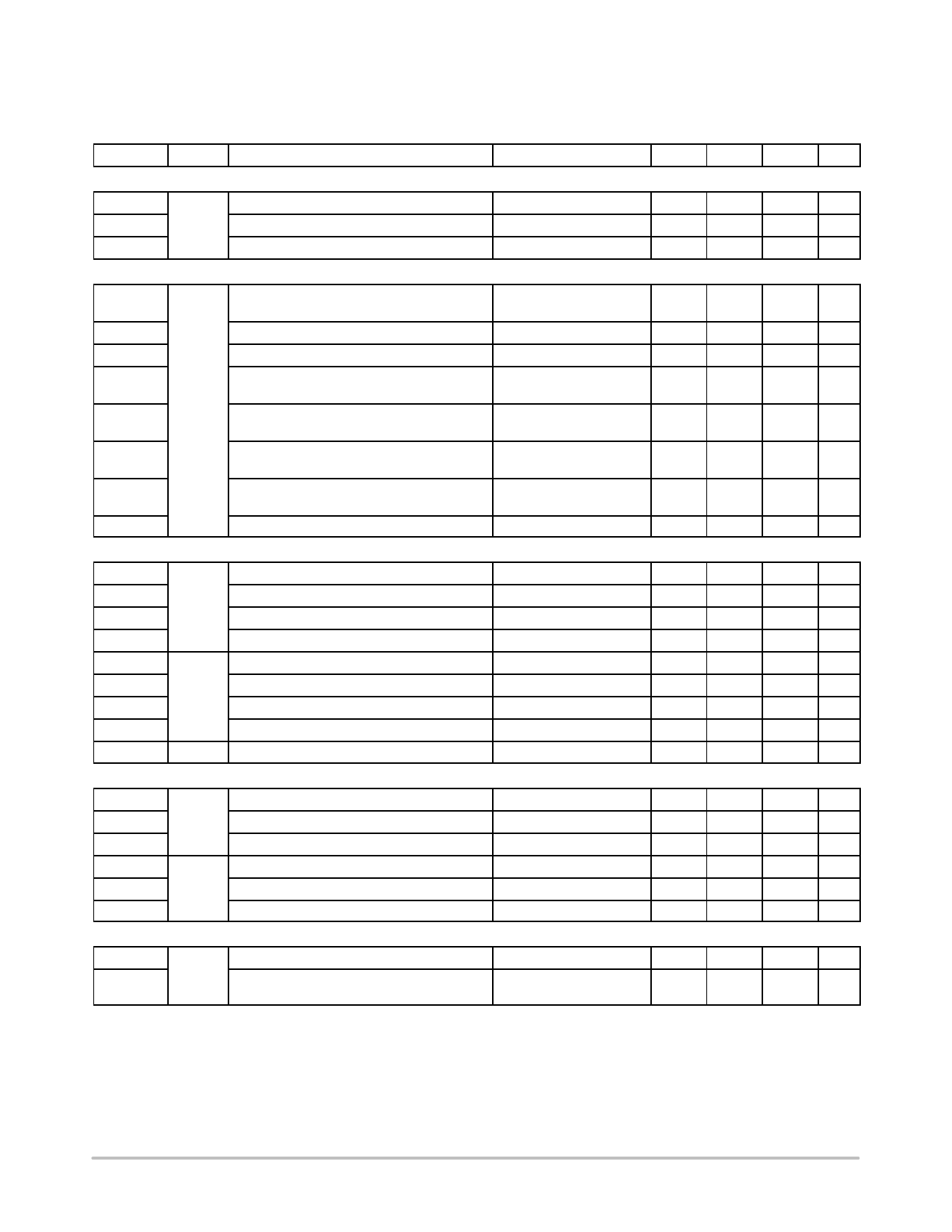
Table 5. DC PARAMETERS
The DC parameters are given for VBB and TJ in the recommended operating ranges unless otherwise specified.
Convention: Currents flowing into the circuit are defined as positive.
Symbol Pin(s)
Parameter
Remark/Test Conditions Min
Typ
Max Unit
Supply Inputs
VBB
IBB
VBB
IBBs
Motordriver
Nominal operating supply range
Total current consumption (Note 9)
Sleep current (Note 10)
Unloaded outputs
6
29
V
15
mA
90
150 mA
IMDmax MOTXP Max peak current through motor coil in normal
300
(Peak)
MOTXN operation
MOTYP
IMDabs MOTYN Absolute error on coil current
At IMDmax, Peak = 300 mA −12
IMDrel
Error on current ratio Icoilx / Icoily
At IMDmax, Peak = 300 mA
−9
Rls
On resistance LOW SIDE driver, high current VBB = 12 V, TJ = 27°C
1.3
range, ambient temperature (Note 11)
mA
12
%
9
%
W
On resistance low side driver, high current
range, high temperature
VBB = 12 V, TJ = 150°C
2.7
3.8
W
Rhs
On resistance HIGH SIDE driver, high current VBB = 12 V, TJ = 27°C
2.0
W
range, ambient temperature (Note 11)
On resistance high side driver, high current
range, high temperature
VBB = 12 V, TJ = 150°C
4.1
5.8
W
Rmpd
Motor pin pulldown resistance
Logic Inputs
VinL
DI, CLK Logic low input level, max
NXT, DIR
VinH
RHB Logic high input level, min
IinL
Logic low input level, max
IinH
Logic high input level, max
VinL
CSB Logic low input level, max
VinH
Logic high input level, min
IinL
Logic low input level, max (Note 8)
IinH
Logic high input level, max (Note 8)
Rpd
TST0 Internal pulldown resistor
Logic Outputs
VOLmax
VOHmax
DO Output voltage when sinking 8 mA
Maximum drain voltage
IOLmax
VOLmax
VOHmax
ERRB
Maximum allowed drain current
Output voltage when sinking 8 mA
Maximum drain voltage
IOLmax
Maximum allowed drain current
Thermal Warning and Shutdown
HiZ Mode
70
kW
Tested at 1 MHz frequency
0.8
V
Tested at 1 MHz frequency 2.4
V
Tested at 1 MHz frequency −1
mA
Tested at 1 MHz frequency
4
mA
Tested at 1 MHz frequency
0.8
V
Tested at 1 MHz frequency 2.4
V
Tested at 1 MHz frequency
−50
mA
Tested at 1 MHz frequency
1
mA
3
9
kW
Pin in open drain state
Pin in open drain state
0.4
V
5.5
V
8
mA
0.4
V
5.5
V
8
mA
Ttw
Ttsd
(Notes 6, 7)
Thermal warning
Thermal shutdown
145
°C
Ttw + 20
°C
6. No more than 100 cumulated hours in life time above Ttw.
7. Thermal shutdown is derived from thermal warning.
8. CSB has an internal weak pullup resistor of 100 kW.
9. Dynamic current is with oscillator running, all analogue cells active. Coil currents 0 mA, SPI active, ERRB inactive, no floating inputs, TST
input tied to GND.
10. All analog cells in powerdown. Logic powered, no clocks running. All outputs unloaded, no floating inputs.
11. Characterization value, not measured in production.
http://onsemi.com
5
Share Link: 