MT9074 Просмотр технического описания (PDF) - Zarlink Semiconductor Inc
Номер в каталоге
Компоненты Описание
производитель
MT9074 Datasheet PDF : 151 Pages
| |||
MT9074
Data Sheet
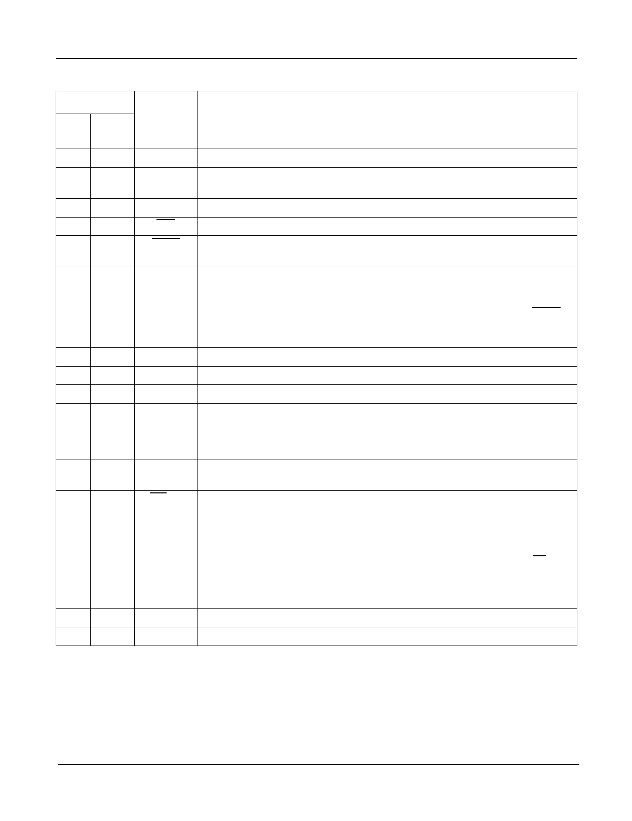
Pin Description
Pin #
68 Pin 100 Pin
PLCC MQFP
Name
Description
56
44
Tdo IEEE 1149.1 Test Data Output. If not used, this pin should be left unconnected.
57
45
Tms
IEEE 1149.1 Test Mode Selection (Input). If not used, this pin should be pulled
high.
58
46
Tclk IEEE 1149.1 Test Clock Signal (Input). If not used, this pin should be pulled high.
59
47
Trst IEEE 1149.1 Reset Signal (Input). If not used, this pin should be held low.
60
48
TxAO Transmit All Ones (Input).High - TTIP, TRING will transmit data normally. Low -
TTIP, TRING will transmit an all ones signal.
61
57
LOS
Loss of signal or synchronization (Output).When high, and LOS/LOF (page 1
address 19 bit 0) is zero, this signal indicates that the receive portion of the
MT9074 is either not detecting an incoming signal (bit LLOS on page 03H address
16H is one) or is detecting a loss of basic frame alignment condition (bit SYNC on
page 03H address 10H is one). If LOS/LOF=1, a high on this pin indicates a loss of
signal condition.
62
58
IC
Internal Connection. Tie to Vss (Ground) for normal operation.
59
NC No Connection. Leave open for normal operation.
63
60
IC
Internal Connection. Tie to VSS (Ground) for normal operation.
64
61 TxDLCLK Transmit Data Link Clock (Output). A gapped clock signal derived from a gated
2.048 Mbit/s clock for transmit data link at 4, 8, 12, 16 or 20 kHz. The transmit data
link data (TxDL) is clocked in on the rising edge of TxDLCLK. TxDLCLK can also
be used to clock DL data out of an external serial controller.
65
62
TxDL
Transmit Data Link (Input). An input serial stream of transmit data link data at 4,
8, 12, 16 or 20 kbit/s.
66
63 S/FR/C1.5i Sychronous/Freerun Extracted Clock (Input): If low, and the internal LIU is
enabled, the MT9074 is in free run mode. Pins 45 C4b and 46 F0b are outputs
generating system clocks. Slips will occur in the receive slip buffer as a result of
any deviation between the MT9074's internal PLL (which is free - running) and the
frequency of the incoming line data. If high, and the internal LIU is enabled, the
MT9074 is in Bus or Line Synchronization mode depending on the BS/LS pin. If
the internal LIU is disabled, in digital framer mode, this pin (C1.5i) takes an input
clock 1.544 Mhz (T1) / 2.048 Mhz (E1) that clocks in the received digital data on
pins RTIP and RRING with its rising edge.
67
64
VDD Positive Power Supply (Input). Digital supply (+5 V ± 5%).
68
65
VSS Negative Power Supply (Input). Digital ground.
Device Overview
The MT9074 in T1 mode operates as an advanced T1 framer with an on-chip Line Interface Unit (LIU) that meets or
supports the recommendations including ITU I.431, AT&T PUB43801, TR-62411, ANSI T1.102, T.403 and T.408.
15
Zarlink Semiconductor Inc.
Share Link: 