MAX3670EGJ Просмотр технического описания (PDF) - Maxim Integrated
Номер в каталоге
Компоненты Описание
производитель
MAX3670EGJ Datasheet PDF : 12 Pages
| |||
Low-Jitter 155MHz/622MHz
Clock Generator
Table 3. Gain Logic Pin Setup
INPUT
PIN
GSEL1
VCC
OPEN
GND
VCC
OPEN
GND
VCC
OPEN
GND
VCC
OPEN
VCC
OPEN
GND
VCC
OPEN
GND
VCC
OPEN
GND
VCC
OPEN
INPUT
PIN
GSEL2
VCC
VCC
VCC
OPEN
OPEN
OPEN
GND
GND
GND
VCC
VCC
VCC
VCC
VCC
OPEN
OPEN
OPEN
GND
GND
GND
OPEN
OPEN
INPUT
PIN
GSEL3
VCC
VCC
VCC
VCC
VCC
VCC
VCC
VCC
VCC
GND
GND
OPEN
OPEN
OPEN
OPEN
OPEN
OPEN
OPEN
OPEN
OPEN
GND
GND
KPD
(µA/UI)
20
20
20
20
20
20
20
20
20
20
20
5
5
5
5
5
5
5
5
5
5
5
DIVIDER
RATIO
N2
1
2
4
8
16
32
64
128
256
512
1024
1
2
4
8
16
32
64
128
256
512
1024
peaking in the PLL passband region to less than 0.1dB.
This can be achieved by setting fZ ≤ K/100.
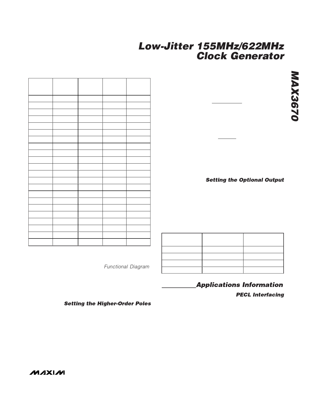
The three-level GSEL pins (see Functional Diagram)
select the phase-detector gain (KPD) and the frequency-
divider ratio (N2). Table 3 summarizes the settings for
the GSEL pins. A more detailed analysis of the loop filter
is located in application note HFDN-13.0 on
www.maxim-ic.com.
Setting the Higher-Order Poles
Spurious noise is generated by the phase detector
switching at the compare frequency, where fCOMPARE
= fVCO/(N1 ✕ N2). Reduce the spurious noise from the
digital phase detector by placing a higher-order pole
(HOP) at a frequency much less than the compare fre-
quency. The HOP should, however, be placed high
enough in frequency that it does not decrease the over-
all loop-phase margin and impact jitter peaking. These
two conditions can be met by selecting the HOP fre-
quency to be (K ✕ 4) < fHOP ≤ fCOMPARE, where K is
the loop bandwidth.
The HOP can be implemented either by providing a
compensation capacitor C2, which produces a pole at
f
HOP=
1
2π(20kΩ)(C2 )
or by adding a lowpass filter, consisting of R3 and C3,
directly on the VCO tuning port, which produces a pole at
f
HOP=
1
2πR3C3
Using R3 and C3 may be preferable for filtering more
noise in the PLL, but it may still be necessary to provide
filtering via C2 when using large values of R1 and N1 ✕ N2
to prevent clipping in the op amp.
Setting the Optional Output
The MAX3670 optional clock output can be set to bina-
ry subdivisions of the main clock frequency. The PSEL1
and PSEL2 pins control the binary divisions. Table 4
shows the pin configuration along with the possible
divider ratios.
Table 4. Setting the Optional Clock
Output Driver
INPUT PIN
PSEL1
VCC
GND
VCC
GND
INPUT PIN
PSEL2
VCC
VCC
GND
GND
VCO TO POUT
DIVIDER RATIO
1
2
4
8
Applications Information
PECL Interfacing
The MAX3670 outputs (MOUT+, MOUT-, POUT+,
POUT-) are designed to interface with PECL signal lev-
els. It is important to bias these ports appropriately. A
circuit that provides a Thévenin equivalent of 50Ω to
VCC - 2V can be used with fixed-impedance transmis-
sion lines with proper termination. To ensure best per-
formance, the differential outputs must have balanced
loads. It is important to note that if optional clock output
is not used, it should be left unconnected to save
power (see Figure 2).
_______________________________________________________________________________________ 9
Share Link: 