TDA5153 Просмотр технического описания (PDF) - Philips Electronics
Номер в каталоге
Компоненты Описание
производитель
TDA5153
Philips Electronics

TDA5153 Datasheet PDF : 28 Pages
| |||
Philips Semiconductors
Pre-amplifier for Hard Disk Drive (HDD)
with MR-read/inductive write heads
Preliminary specification
TDA5153
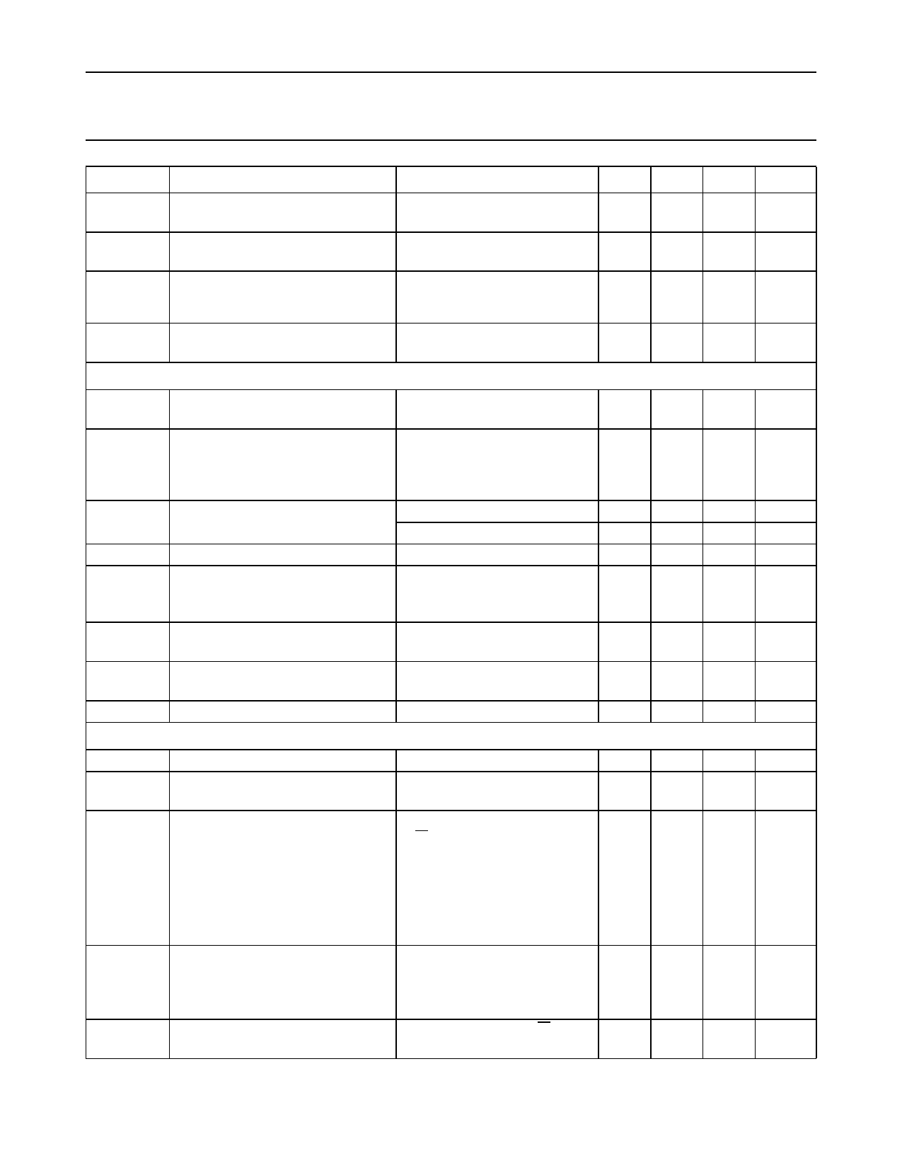
SYMBOL
PARAMETER
CONDITIONS
MIN. TYP. MAX. UNIT
Io(max)(dif)
Vo(cm)
∆--∆---V-V---o-C-c--C-m--
maximum differential output
current
common mode output voltage in
read mode
RDx, RDy
common mode DC supply rejection
in read mode
−
4
−
mA
1.0 1.5 2.0 V
−
20
−
dB
Zo(n)(dif)
differential output impedance in
other modes (write, standby, sleep)
−
50
−
kΩ
Write characteristics
IWR
∆IWR
Vs(max)(p-p)
Ro(dif)
tr, tf
tas
tpd
αcs
write current adjust range (in the
write drivers)
tolerance (excluding Rext);
-I-W-----R-I--R--–--W--I--R-(--P-W--R---)(--P---R---)
maximum voltage swing
(peak-to-peak value)
differential output resistance
write current rise/fall time without
flip-flop (10% to 90%); note 8
write current asymmetry; note 9
propagation delay 50% of
(WDIx/WDIy) to 50% of (Wx, Wy)
channel separation
Rext = 10 kΩ; 1 mA steps
20
IWR(PR) = 35 mA
−
VCC(WD) = 5 V
−
VCC(WD) = 8 V (differential)
−
−
VCC(WD) = 8 V; Lh = 150 nH,
−
Rh = 10 Ω; IWR = 35 mA;
f = 20 MHz
percentage of tr/tf
−
(tr, tf and logic asymmetry)
write head short circuited; data −
flip-flop by passed
unselected head
−
35
51
mA
±7
−
%
−
8
V
−
13
V
200 −
Ω
−
1.8 ns
−
5
%
−
5
ns
45
−
dB
Switching characteristics
fSCLK
∆Vo(cm)
trec(W-R)
tsw(R)
toff(R)
serial interface clock rate
−
output common mode DC voltage IMR = 10 mA; IWR = 35 mA
−
change from Read to Write modes
write to read recovery time
(AC and DC settling); note 10
from 50% of the rising edge of
R/W to steady state read-back
signal: AC and DC settling at
90% (without load at
RDx − RDy)
read amplifier OFF: d5 = 0 −
read amplifier ON: d5 = 1 −
head switching (in read mode),
standby to read active and MR
current change recovery time;
(AC and DC settling); note 11
from falling edge of SEN to
−
steady state read-back signal;
(without load at RDx − RDy)
read amplifier off time
from falling edge of R/W to
−
read head inactive
−
25
200 −
MHz
mV
3
4.5 µs
100 150 µs
3
4.5 µs
−
50
ns
1997 Jul 02
20
Share Link: