TDA5153 Просмотр технического описания (PDF) - Philips Electronics
Номер в каталоге
Компоненты Описание
производитель
TDA5153
Philips Electronics

TDA5153 Datasheet PDF : 28 Pages
| |||
Philips Semiconductors
Pre-amplifier for Hard Disk Drive (HDD)
with MR-read/inductive write heads
Preliminary specification
TDA5153
8.10.5.3 Thermal asperity detector
d2 = logic 1, d1 = don’t care, d0 = either logic or 1. Unlike
the above tests, the thermal asperity detection does not
use the RDx to RDy outputs. Thus, the reader is fully
operational. In case a thermal asperity is detected, it is
flagged at the HUS pin.
The threshold voltage for the thermal asperity detection is
2-bit programmable. These 2 bits consist of d0 (LSB) of
the test mode register (address = 0XXX0110), as the
MSB, and b2 of the compensation register
(address = 0XXX0111).
Vth = (210 + 560 ⋅ d0 + 280 ⋅ b2) µV ,
where d0 is d0 of test mode register and b2 is d2 of
capacitor compensation register.
8.10.6 WRITE AMPLIFIER PROGRAMMABLE CAPACITORS
By default (d2 = d1 = d0 = logic 0) the programmable
capacitors are zero. These capacitors are used to improve
the performance of the write amplifier according to the
write amplifier output load.
attenuator provides a pole which limits the bandwidth and
reduces the high-frequency noise. The HF pole can be
used in combination with the HF zero in order to boost the
HF gain locally and yet limit the very high frequency noise
enhancement.
8.10.8 HIGH FREQUENCY GAIN BOOST REGISTER
By default (d3 = d2 = d1 = d0 = logic 0), the high
frequency gain boost is not active. The gain boost provides
a zero which allows to optimize the bandwidth of the read
amplifier and to correct for attenuation caused by series
inductances in the leads between the MR-heads and the
read amplifier inputs.
8.10.9 SETTLE PULSE
By default (d2 = d1 = d0 = logic 0) the settle pulse has a
nominal duration of 3 µs. Its value can be programmed
from 2.125 µs to 3 µs according to the following formula:
tst = 2 + -(---4-----⋅---d----2-----+-----2----⋅---d---1-1-----+-----1-----⋅---d----0----+-----1----)- µs
8.10.7 HIGH FREQUENCY GAIN ATTENUATOR POLE
REGISTER
By default (d3 = d2 = d1 = d0 = logic 0), the high
frequency gain attenuator is not active. The gain
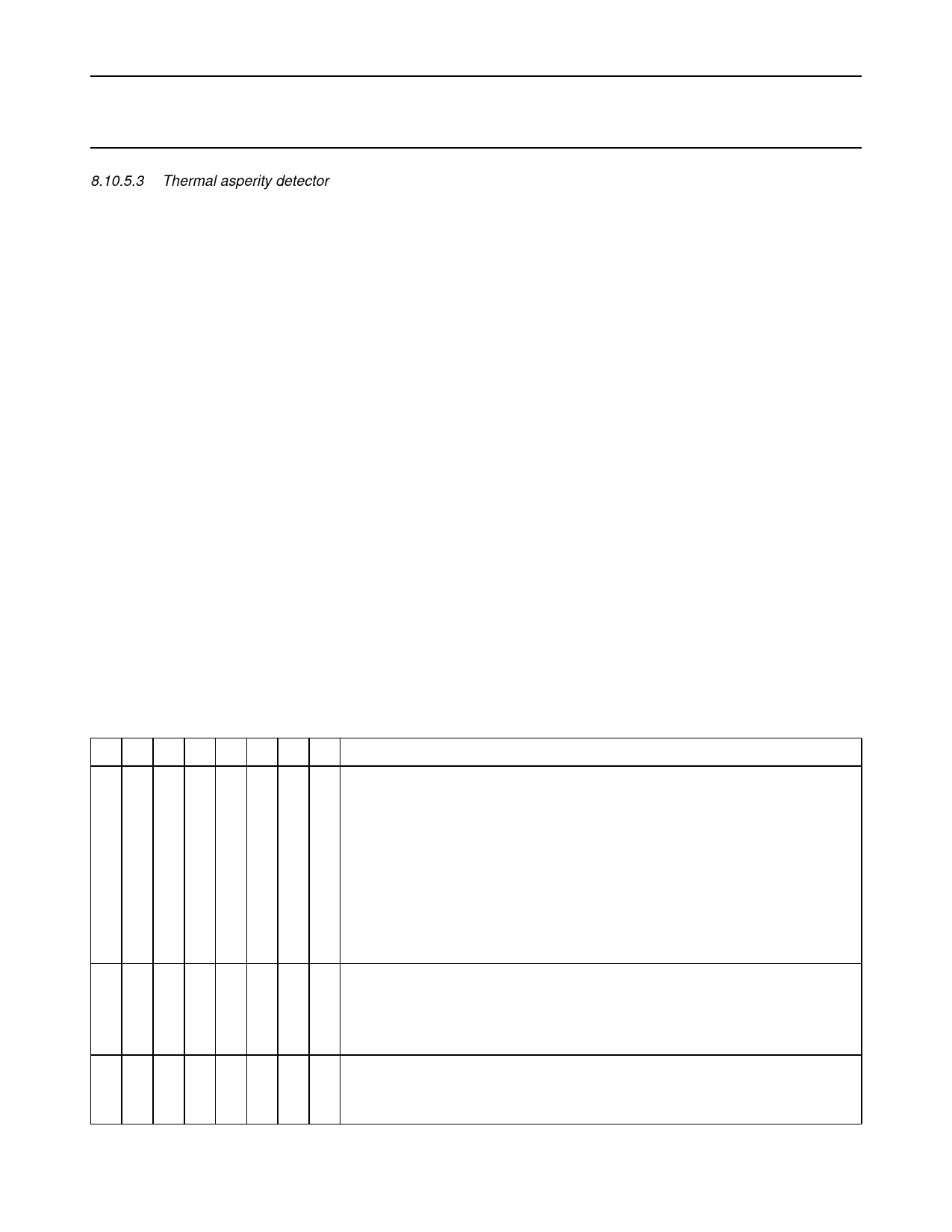
8.10.10 ADDRESS REGISTERS; note 1
A7 A6 A5 A4 A3 A2 A1 A0
DESCRIPTION
0 0 0 0 0 0 1 0 configuration register:
d0 = 0: use data flip-flop; d0 = 1: by-pass data flip-flop
d1 = 0: the WDI inputs are PECL levels; d1 = 1: invalid
d2 = 0: write current inhibit active; d2 = 1: write current inhibit inactive
read mode: d3 = 0: HUS active; d3 = 1: HUS HIGH
write mode: d3 = 0: HUS active; d3 = 1: HUS LOW
d4 = 0: read gain nominal; d4 = 1: read gain nominal + 3 dB
d5 = 0: read amplifier OFF during write mode; d5 = 1: read amplifier ON
during write mode
0 0 0 1 0 0 1 0 power control register:
(d1, d0) = (0, 0): sleep mode
(d1, d0) = (1, 0) or (0, 1): standby mode
(d1, d0) = (1, 1): active mode (write or read)
0 0 1 0 0 0 1 0 head select register:
6 channels: (d2,d1,d0) = (0,0,0) to (1,0,1): H0 to H5
4 channels: (d2,d1,d0) = (0, 0, 1) to (1, 0, 0): H1 to H4
1997 Jul 02
14
Share Link: