IP101A Просмотр технического описания (PDF) - Unspecified
Номер в каталоге
Компоненты Описание
производитель
IP101A Datasheet PDF : 36 Pages
| |||
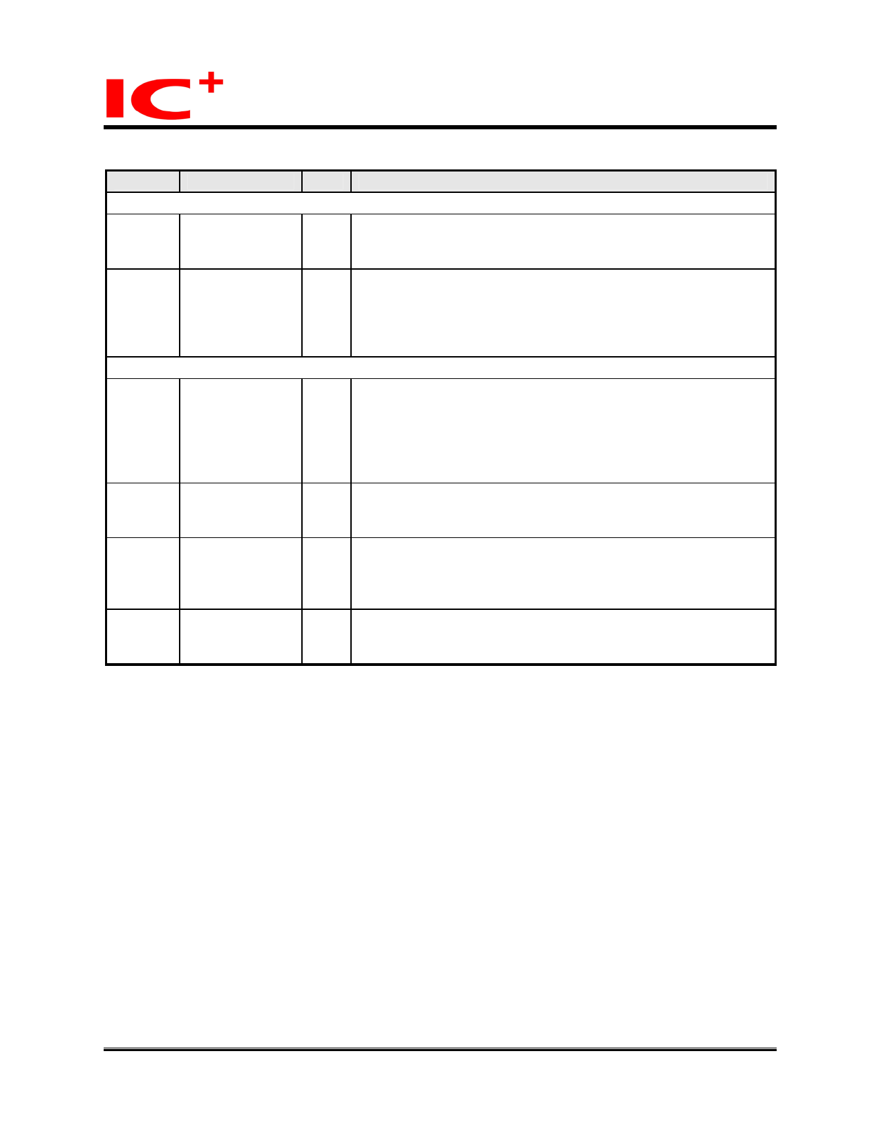
Pin Descriptions (continued)
IP101A LF
Data Sheet
Pin no. Label
Type Description
Clock and Miscellaneous - Crystal Input/Output Pins
47 X2
O 25MHz Crystal Output: Connects to crystal to provide the
25MHz output. It must be left open when X1 is driven with an
external 25MHz oscillator.
46 X1
I 25MHz Crystal Input: Connects to crystal to provide the 25MHz
crystal input. If a 25MHz oscillator is used, connect X1 to the
oscillator’s output. If a 50MHz clock is applied to pin7, X1 should
be connected to VSS or 2.5v VDD. Please refer to the clock
source description.
Clock and Miscellaneous - Miscellaneous Pins
42 RESET_N
I RESET_N: Enable a low status signal will reset the chip. For a
complete reset function. 25MHz clock (x1) must be active for a
minimum of 10 clock cycles before the rising edge of RESET_N.
Chip will be able to operate after 2.5ms delay of the rising edge
of RESET_N. The 2.5ms extention is to ensure the stability of
system power.
48
INTR
O Interrupt Pin: When the MII register 17:<15> is set to high, this
(OD) pin is used as an interrupt pin (Notice: this is an open drain
output, so an external pulled-up resistor is needed)
27 TEST_ON
(PD)
Test Enable: Set this pin to high to enable test mode, while for
normal operation, this pin does not need to be connected. (An
internal weak pulled-down is used to disable test mode as a
default)
28 ISET
I Transmit Bias Resistor Connection: This pin should be
connected to GND via a 6.2KΩ (1%) resistor to define driving
current for transmit DAC.
Copyright © 2004, IC Plus Corp.
11/36
Oct 22, 2007
IP101A LF-DS-R12
Share Link: 